
The in-band full-duplex technique is regarded as a potential solution for significantly enhancing spectrum efficiency in the next generation communication system (5G). The biggest challenge in achieving full-duplex communication is overcoming self-interference from the simultaneous use of the same frequency band for transmission and reception. A novel RF cancellation circuit with direct RF correlative detection is automatically adjusted in real-time to optimize cancellation. Measured results show that the cancellation circuit provides greater than 50 dB of Tx-to-Rx isolation over a 50 MHz bandwidth. Moreover, the design is an independent module which can readily be cascaded for MIMO scenarios.
The 4th generation communication system (4G) has begun commercialization and is reaching maturity. Technical solutions and standards for the next generation communication system (5G) are now attracting the attention of developers around the world.1 Future support for the explosive growth of data traffic and the massive increase in the number of interconnected devices is the main driver behind 5G; thus, developments to fully exploit potential spectrum resources and to enhance spectrum efficiency are essential.
In-band full-duplex communications has been widely regarded as a potential solution to improve the spectrum efficiency of wireless systems.2,3 Current systems employ either time division duplexing (TDD) or frequency division duplexing (FDD) to achieve bidirectional communication. In these systems, high Tx-to-Rx isolation is realized with different time slots or frequency bands for transmission and reception. Using the in-band full-duplex communication technique, however, a radio can simultaneously transmit and receive over the same frequency band, enabling a wireless network to double its spectrum utilization.
There have been several recent attempts to build this type of full-duplex transceiver4-7 but, its practical realization is still subject to many challenges. The main one is strong self-interference from the transmit side of the node. Therefore, the principal objective for a full-duplex design is to suppress self-interference as much as possible.
The block diagram of a basic full-duplex transceiver with RF and digital cancellation is shown in Figure 1. Compared to a traditional transceiver, an additional RF or analog cancellation circuit is used to eliminate self-interference. About 63 dB of Tx-to-Rx isolation across an 80 MHz bandwidth was obtained in the analog domain by Bharadia et al.7 This was accomplished with an intricate 16-tap canceller composed of tunable attenuators and delay lines along with a complex cancellation control algorithm. RF cancellation can provide significant isolation to avoid receiver saturation or analog-to-digital converter overload caused by strong self-interference. Moreover, it may be augmented with digital cancellation.
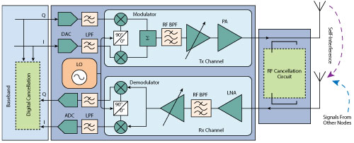
Figure 1 Block diagram of a separated-antenna, full-duplex transceiver with an independent RF cancellation module.
This article introduces a novel RF cancellation technique with direct RF correlative detection. This is realized with an independent RF module that automatically adjusts phase and magnitude to optimize cancellation. The direct RF correlative detection method can significantly reduce hardware and adaptive algorithm complexity compared with other designs.6,7 Correlative detection employed in this design also has several advantages as compared to the power detection method.4 Power detection utilizes only the strength of received signals, and thus may be easily disturbed by other interference, while correlative detection will not. Correlative detection provides both the magnitude and phase information of self-interference so that an adaptive adjustment algorithm (such as the LMS algorithm) can be easily implemented. Finally, the RF cancellation module used in correlative detection can readily be cascaded to support MIMO systems.
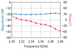
Figure 2 Measured response from separated transmit and receive antennas in a typical laboratory environment.
CIRCUIT DESIGN
Frequency Response of Self-Interference Channel
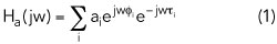
In the separated-antenna based full-duplex transceiver, self-interference consists of two components: the self-interference propagating directly from the transmit to the receive antenna, and reflected components from nearby scatter. The frequency response of self-interference in a separated-antenna architecture can be written as:
where i = 0 denotes the frequency response of the direct path from transmit antenna to the receive antenna, and i = 1,2,3 denotes the frequency response of multipath scattering. aiejwϕi represents the magnitude and phase information and τi is the time delay for each path. As shown in Figure 2, a non-flat frequency response caused by multipath reflection is observed in a typical environment.
The self-interference signal at the receive side looks different from transmitted signal at the Tx antenna due to the non-flat frequency response, especially when a wideband modulation signal is transmitted. For this reason, it is quite difficult to obtain a perfect inverse of self-interference for RF cancellation. As a result, RF cancellation is imperfect. Despite this, RF cancellation is necessary because: 1) It provides high transmit-to-receive isolation, enough to prevent the receiver from saturating; 2) RF cancellation is unaffected by phase noise of the transceiver local oscillator; 3) RF cancellation using the transmit signal after the power amplifier as the reference can eliminate nonlinear self-interference due to power amplifier nonlinearity.
RF Cancellation Design with Correlative Detection
In this work, we consider an RF cancellation design for a separated-antenna full-duplex transceiver architecture. A simplified block diagram is shown in Figure 3. The RF cancellation circuit is implemented as an independent RF module which can be divided into two parts: 1) a cancellation unit consisting of a vector modulator, a transmission delay line, several RF amplifiers a directional coupler and other supporting components, and 2) a correlative detection unit consisting of a directional coupler, an RF multiplier, a quadrature demodulator and several RF amplifiers.
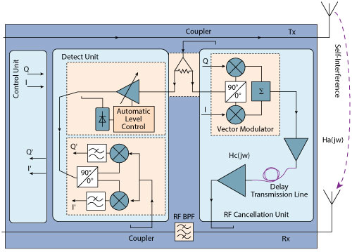
Figure 3 Block diagram of an RF cancellation circuit with direct RF correlative detection.
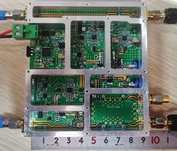
Figure 4 RF cancellation module.
In the cancellation unit, the vector modulator is used as a programmable phase shifter and attenuator to generate a replica of the self-interference signal. It provides fine-grained control to match amplitude and phase for the inverted signal path. Cancellation that inverts a signal through phase adjustment only, however, will always have a bandwidth constraint. To obtain the inverse for wideband signals, a fixed delay transmission line is used to achieve the same group delay in the inverted and self-interference paths.
Correlative detection of the self-interference signal is accomplished in the detection unit. A quadrature demodulator with low-pass filters at the baseband ports acts as a direct RF correlative detector. Considering that the power level of the reference signal at the LO port of the demodulator must be controlled within a suitable range, an automatic power level control loop is constitutive with the RF multiplier, directional coupler, log detector and operational amplifier to provide a reference signal with a constant power level.
The transmitted signal is passed through the transmit channel interface of the RF cancellation module to the transmit antenna and is also coupled and split into two parts to form reference signals for the RF cancellation and detection units. The RF cancellation unit generates an inverted replica of the self-interference signal for elimination at the receive side. Residual signal is fed to the quadrature demodulator for correlative detection. The output is sampled to obtain self-interference magnitude and phase information for cancellation adjustment. Figure 4 shows the completed RF cancellation module.
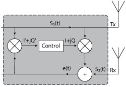
Figure 5 RF cancellation system model.
The RF cancellation system model is shown in Figure 5. The complex transmitted signal is denoted by s1(t), and s2(t) is the received signal at the receive antenna. The output of the receive channel can be written as:

where I + jQ is the baseband input of the vector modulator for amplitude and phase adjustment of self-interference.
The complex output of the correlative detection unit is given by:

The goal of self-tuning is to set the complex amplitude I + jQ such that self-interference is minimized. The adaptive least mean square (LMS) algorithm can be easily realized in this RF cancellation implementation. The gradient vector of the LMS algorithm is:
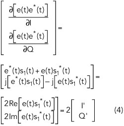
where Re[·] represents the real part and Im[∙] represents the imaginary part.
The formula for the LMS algorithm can be written as follows:
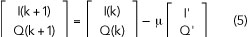
where μ denotes a step size.
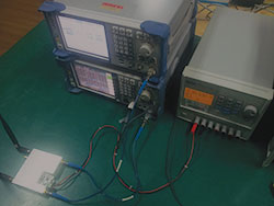
Figure 6 Setup for measuring RF self-interference cancellation performance.
Note that in a practical cancellation circuit, a constant phase displacement ϕ between the reference signal of the detection unit and the signal in the cancellation unit is measured and calibrated, so the formula of the LMS algorithm is rewritten as follows:
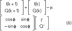
The output of correlative detection part I’ + jQ is sampled for each iteration and the complex amplitude of the cancellation unit I + jQ is calculated according to Equation 6. This RF cancellation implementation using the LMS algorithm can automatically adjust the phase and amplitude in real time to optimize self-interference cancellation.
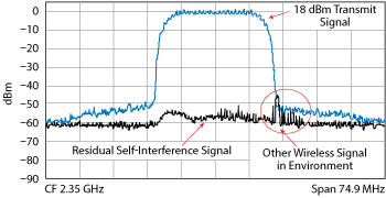
Figure 7 Cancellation at 2.35 GHz with a 20 MHz modulation signal.
EXPERIMENTAL RESULTS
The RF cancellation module with real-time adaptive cancellation is evaluated in a laboratory environment (see Figure 6). A Rohde & Schwarz (R&S) SMBV100A vector signal generates wideband digital modulation signals at a center frequency of 2.35 GHz with an average power of 18 dBm. The output is connected directly to the Tx channel of the RF cancellation module and transmitted with an omni-directional antenna. Another omni-directional antenna is employed as the receive antenna. Signals are observed with a Rohde & Schwarz FSL6 spectrum analyzer on the Rx side. Tx-to-Rx isolation for optimal cancellation is measured using a Keysight N5230A vector network analyzer (VNA).
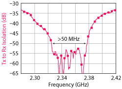
Figure 8 Tx-Rx isolation measured at optimal cancellation.
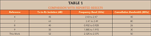
Adaptive RF cancellation at a 2.35 GHz center frequency with a 20 MHz bandwidth QAM-16 modulation signal is shown in Figure 7. Residual self-interference is about -38 dBm at an average transmit power of 18 dBm. Thus, a total of 56 dB of self-interference suppression is achieved with the RF cancellation module. To evaluate bandwidth performance, S-parameters between the Tx and Rx ports of the module are measured in the optimum cancellation state. As is shown in Figure 8, the RF cancellation module provides greater than 50 dB Tx-to-Rx isolation across a 50 MHz bandwidth. Table 1 shows how this compares with other published approaches.
CONCLUSION
A practical RF cancellation circuit employs adaptive cancellation adjustment in real time using direct RF correlative detection. Experimental results show that it provides greater than 50 dB isolation over a 50 MHz bandwidth. Using correlative detection, good real-time adaptive adjustment is achieved. To build a practical full-duplex radio, however, further suppression is required through digital cancellation. With this circuit and algorithm, transmit interference can be reduced significant so that the IF circuit and the digital circuit can process the received signal with little difficulty. For MIMO, this independent RF cancellation module can be readily cascaded to cancel interference from other antennas.
ACKNOWLEDGMENT
This work is supported in part by the National Natural Science Foundation of China (NSFC) under Grant 61401093.
References
- J. G. Andrews, S. Buzzi, W. Choi, S. Hanly, A. Lozano, A. C. K. Soong and J. C. Zhang, “What Will 5G Be?,” IEEE Journal on Selected Areas in Communications, Vol. 32, No. 6, June 2014, pp. 1065–1082.
- S. Hong, J. Brand, J. Choi, M. Jain, J. Mehlman, S. Katti and P. Levis, “Applications of Self-Interference Cancellation in 5G and Beyond,” IEEE Communications Magazine, Vol. 52, No. 2, February 2014, pp. 114–121.
- C. Rowell, S. Han, Z. Xu and I. C. Lin, “Green RF Technologies for 5G Networks,” IEEE International Wireless Symposium, March 2014, pp. 1–4.
- M. Jain, J. I. Choi, T. M. Kim, D. Bharadia, S. Seth, K. Srinivasan, P. Levis, S. Katti and P. Sinha, “Practical, Real-Time, Full Duplex Wireless,” Proceedings of the 17th Annual International Conference on Mobile Computing and Networking, September 2011, pp. 301–312.
- J. I. Choi, M. Jain, K. Srinivasan, P. Levis and S. Katti,“ Achieving Single Channel, Full Duplex Wireless Communication,” Proceedings of the 16th Annual International Conference on Mobile Computing and Networking, September 2010, pp. 1–12.
- D. Korpi, T. Huusari, Y. S. Choi, L. Anttila, S. Talwar and M. Valkama, “Full-Duplex Mobile Device-Pushing The Limits,” arXiv:1410.3191v1 [cs.IT], October 2014.
- D. Bharadia, E. McMilin and S. Katti, “Full Duplex Radios,” Proceedings of the ACM SIGCOMM Conference, August 2013, pp. 375–386.
- M. E. Knox, “Single Antenna Full Duplex Communications Using a Common Carrier,” IEEE Conference on Wireless and Microwave Technology, April 2012, pp.1–6.
- L. Laughlin, M. A. Beach, K. A. Morris, and J. L. Haine, “Optimum Single Antenna Full Duplex Using Hybrid Junctions,” IEEE Journal on Selected Areas in Communications, Vol. 32, No. 9, June 2014, pp.1653–1661.