
Adaptive Feedforward Linearization For RF Power Amplifiers
Shawn P. Stapleton
Simon Fraser University, School of Engineering Science
Burnaby, B.C., Canada
The design of RF power amplifiers has become increasingly complex. With modern radio communications systems focusing on ever-higher data rates and better spectral efficiencies, these challenges to amplifier design will continue. Modulation schemes such as multilevel linear quadrature amplitude modulation (QAM) increase spectral efficiency yet their operating envelopes fluctuate, making this approach much more sensitive to the inherent nonlinear component of power amplifier behavior - the major source of nonlinear distortion in microwave transmitters. The traditional approach to the distortion problem is to back off the output power of a class A power amplifier until it operates within a linear region and distortion is reduced to an acceptable level (that is, where average output power is much smaller than saturation power). Unfortunately, this course of action increases cost and reduces efficiency for amplifier design.
As supplementary stages are added to allow the amplifier to maintain transmitted power levels, more DC power is consumed. Further, with efficiency so critical for battery-operated systems and designs with limited enclosure space for heat dissipation, linearization of a power-efficient class AB amplifier is a much more desirable alternative to backing off output power. Class AB power amplifiers provide approximately 25 percent efficiency and are more power efficient than class A amplifiers, which only attain approximately five percent efficiency. Class AB amplifiers also exhibit gain roll off at low input powers and at saturation.
The industry continues to embrace linear modulation techniques such as quadrature phase-shift keying (QPSK), 64-state QAM (64QAM) and multicarrier configurations. As this trend continues, active linearization of the power amplifier will remain a key technology for reducing nonlinear distortions. The transmitted signal from one of these modern linear modulation schemes may exhibit a fluctuating envelope, which generates intermodulation (IM) distortion in the power amplifier. Today's digital communication systems typically use very narrow channel spacing and require better distortion performance than analog systems. Since most of the IM power appears as interference in adjacent channels, it is critical that these systems utilize a highly linear power amplifier.
Unfortunately, power amplifiers are devices that exhibit both linear and nonlinear behavior, and these characteristics have a tendency to change over time due to repeated exposure to temperature changes, voltage variations, channel changes and aging. Therefore, any robust linearization approach must incorporate the capacity for adaptability. Adaptive feedforward linearization represents just such an approach - one that has the distinct advantage of being able to handle wide bandwidths while continuously adjusting for component drift and power level changes.
Design Challenges
Power amplifier nonlinearity is typically characterized by amplitude-dependent gain variation (AM/AM) and amplitude-dependent phase shift (AM/PM). However, in addition to nonlinearities, RF amplifiers also possess memory, that is, the output signal depends on the current value of the input signal as well as previous input values spanning the memory of the amplifier.
Other design constraints are the result of regulatory bodies, which specify power spectral density masks defining the maximum allowable adjacent-channel interference (ACI) levels. For example, Figure 1 shows the application of a mask specified by the trans-European terrestrial trunked radio (TETRA) standard that uses a p/4 differential QPSK (DQPSK) modulation format with a symbol rate of 18 kHz and channel spacing of 25 kHz. A class AB power amplifier operating at a back-off power of 3 dB is shown superimposed on the mask to illustrate how the distorted output falls outside the specification.
Feedforward Linearization
The idea of using negative feedback for linearizing amplifiers is not new. First described in 1927 by H.S. Black of Bell Telephone Laboratories,1 the concept of feedforward is simple. If the amplifier output is reduced to the same level as the input, the difference between the input and output is only the distortion generated by the amplifier. Further, if this resulting distortion is then amplified using a different amplifier and subtracted from the original amplifier output, theoretically only a linear amplification of the input signal remains.
 Figure 2 shows a schematic illustrating the key components of the feedforward linearizer circuit. Feedforward linearization really utilizes two circuits: an input signal cancellation circuit and a distortion (or error) cancellation circuit. The incoming signal is split into two paths. The upper path, or signal-cancellation circuit, contains a complex gain adjuster and primary power amplifier. The signal-cancellation circuit's complex gain adjuster alters the amplitude and phase so that the input reference signal is cancelled from the primary power amplifier's output, leaving an error signal that contains both the linear and nonlinear components of the amplifier distortion.
The second path, or error-cancellation circuit, carries a replica of the primary output with the amplified signal plus distortion but with latency added to match the delay in the upper path. The distortion-only signal from the upper path is fed to the lower path. There the signal is amplitude and phase adjusted by a complex gain adjuster and combined with the delayed power amplifier's output, eliminating the distortion. The linear distortion component is due to deviations of the amplifier's frequency response from flat gain and linear phase.2 Note that distortion from memory effects also can be compensated using the feedforward technique since these effects are included in the error signal.
Looking again at the diagram, the values for the sampling coupler and fixed attenuation should be chosen to match the gain of the primary amplifier. Variable attenuation is included in the circuit to enable the output level to be precisely adjusted to match the input reference, while the variable phase shifter adjusts the power amplifier output in an antiphase arrangement with the input reference. The delay line in the error-cancellation branch of the circuit is necessary for wide-bandwidth operation and compensates for the group delay of the primary amplifier by time aligning the power amplifier output and reference signals before they are combined. The error-cancellation circuit is used to suppress the distortion component of the power amplifier output, leaving only the linear-amplified component of its output signal. In order to suppress the distortion component of the signal, the gain of the power amplifier used in the error-cancellation circuit must be carefully chosen to match the sum of the effects of the sampling coupler, fixed attenuator and output coupler. Thus, the error signal is amplified to approximately the same level as the distortion component in the power amplifier output signal.
Since feedforward linearization is based on subtracting nearly equal quantities in the signal-cancellation loop, its major parameters must adapt to changes in the operating environment. In the mid-'80s and early '90s, many patents covering adaptive feedforward systems were filed. These patents encompass two general methods of adaptation, both with and without the use of pilot tones. The first is an adaptation based on power minimization;3 the second is an adaptation based on gradient signals.4
The control scheme for power minimization adaptation is based on trying to adjust the complex-vector modulator in the signal-cancellation circuit. Theoretically, this process minimizes the measured power of the error signal in the frequency band occupied by the reference signal. The frequency range chosen for the error-cancellation circuit includes only the bands occupied by the distortion. Once the optimum parameters have been achieved, deliberate perturbations are required to continuously update the coefficients, which reduces the effects of IM distortion suppression.
Adaptive feedforward based on the use of gradient signals requires a continuous computation to estimate the gradient of a three-dimensional power surface. The surface for the signal-cancellation circuit consists of the power in the error signal. This power is minimized when the reference signal is completely suppressed, leaving only distortion. The surface for the error-cancellation circuit is the power in the linearizer-output signal, and the power is minimized when the distortion is completely suppressed from the primary power amplifier's output signal. Since the gradient is continually computed, no deliberate misadjustment is required.
A Gradient Adaptation Feedforward Linearizer Example
Figure 3 shows an example circuit schematic for the error-cancellation loop in a feedforward linearizer based on the gradient-adaptation method created by the Hewlett-Packard Advanced Design System (HP ADS). A rectangular implementation is used for the complex gain adjuster. The input is of a two-tone modulation with the following specifications: Ka = -0.1 adaptation rate and Kb = -0.01 adaptation rate. A rectangular vector modulator is used, and the circuit operates at 5 dB back off from the 1 dB compression point. Ideal passive components are assumed.
When implementing this circuit, care must be taken in the choice of adaptation parameters. The best approach is to ensure that the signal-cancellation loop (a adaptation coefficient) has converged to within a small variance before the error-cancellation loop (b adaptation coefficient) begins to converge.
When gradient-based adaptation is used, delay must be added to the upper branch of the error-cancellation loop to ensure proper cancellation. If feasible, a bandstop filter may be incorporated after the output coupler to reduce the linear portion of the output signal. This configuration effectively speeds up the adaptation process. If the power minimization method is employed, then a bandpass filter is used to sample the output IM distortion.
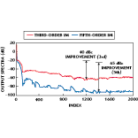 Figure 4 shows the level of improvement exhibited in both third- and fifth-order IM levels at the output of the feedforward linearizer in the first simulation. In the example, the signal-cancellation loop is allowed to converge before the error-cancellation loop is turned on to avoid instability. This condition can occur if close attention is not paid to the adaptation procedure. The error-cancellation loop takes more
 time to optimize than the signal-cancellation loop because of the order of magnitude difference in adaptation rates. Taking the example a step further, if the power amplifier is driven using 5 dB of back off, high levels of IM power and harmonics are generated. Figure 5 shows the resulting output once the coefficients have adapted.
Conclusion
As the duties of RF power amplifiers become increasingly complex, innovative approaches must be developed to minimize distortion. Adaptive feedforward linearization, while based on a concept developed many years ago, represents an optimized approach to solving the problem of IM distortion in multichannel, wideband applications. The linearization example presented here demonstrates the kind of performance that can be achieved with feedforward linearization. System-level simulation provides a solid starting point for carrying out an implementation quickly since designed components can be integrated into the system to gauge the impact on overall performance.
References
1. H.S. Black, "Inventing the Negative Feedback Amplifier," IEEE Spectrum, December 1977, pp. 55-60.
2. H. Seidel, "A Microwave Feedforward Experiment," Bell Systems Technical Journal, Vol. 50, No. 9, November 1971, pp. 2879-2918.
3. M.G. Oberman and J.F. Long, "Feedforward Distortion Minimization Circuit," U.S. Patent 5,077,532, December 31, 1991.
4. J.K. Cavers, "Adaptation Behavior of a Feedforward Amplifier Linearizer," IEEE Transactions on Vehicular Technology, Vol. 44, No. 1, February 1995, pp. 31-40.
Shawn P. Stapleton has 17 years of experience in RF and microwave circuit and systems design. He is currently a professor of electrical engineering at Simon Fraser University in Burnaby, British Columbia, Canada, as well as a consultant for HP EEsof. He has developed GaAs MMIC components, including mixers, amplifiers, frequency dividers and oscillators. His most recent projects include digital signal processing, mobile communications and RF/microwave systems.