
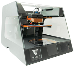
Figure 1 Low-cost Voxel8 Developers Kit 3D printer. Picture is taken from the Voxel8 website.1
The MITRE Corporation is investigating the potential of a new generation of additive manufacturing (AM), commonly known as 3D printing, to realize complex geometries of wideband phased array and metamaterial designs using low-cost, compact, desktop printers. Samples of the 3D printed plastic and conductive ink printed at room temperature were characterized over frequency. The polylactic acid (PLA) dielectric constant and loss tangent are found to be stable up to 18 GHz. The PLA internal architecture was varied to achieve lower effective dissipation factors, which extends usefulness to high frequency applications. Microstrip line samples were fabricated with simulated and measured insertion loss data validating the high conductivity through millimeter wave frequencies. A 3D printed monopole Wi-Fi antenna was built and tested. The measured gain patterns showed excellent agreement with the computational electromagnetic model. The next step is to build and test a complex, electrically-functional phased array and a complex metamaterial structure, and verify simulation through measurement.
There has been increasing demand from the defense and intelligence communities to come up with creative ways to put urgently needed capabilities into the hands of warfighters in a very short time with a combination of lower cost, smaller form factor and covertness in mind. To meet these challenges with agility, the ability to achieve both metallic patterning and polymer deposition in a single, automated process from a low-cost 3D printer has opened the door for the next-generation of rapid prototyping systems. The MITRE Corporation, with the help of 3D printer manufacturer Voxel8, is investigating the applicability of multi-material additive manufacturing, or 3D printed electronics, for high-performance antennas and RF devices. Figure 1 shows the Voxel8 3D printer used for these experiments.
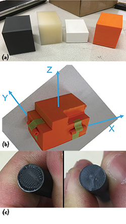
Figure 2 3D printed cubes, realized from four different colored PLA spools (a), machined dielectric sleeves cut out from different side of the cube: XZ and YZ planes (b), and cylinders printed in the XY plane with rectilinear infill (left) and concentric infill (right)(c).
Material Characterization
In order to design antennas and RF circuits, well defined electrical properties within the frequency band of operation are needed. The dielectric material was characterized by measuring a 3D printed dielectric sleeve in a 7 mm coaxial airline standard.2 A variety of samples were tested to investigate effects of different pigments, print orientations and in fill density (see Figure 2).
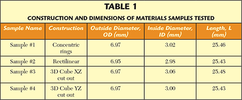
First a solid cube was 3D printed from four different colors of PLA filament. Then solid cylinders from different orientations were cut out to test print orientations. Solid cylinders were also printed using rectilinear and concentric rings to test effects of infill patterns. Next, all cylinders were machined to have specific inner diameter, outer diameter and sample length to fit inside the coaxial airline test fixture shown in Figure 3. Table 1 shows the construction and dimensions of each sample.
The permittivity and loss tangent were measured using a Keysight network analyzer loaded with a material characterization software.3 The reflection/transmission permeability and permittivity polynomial fit technique was used. This technique best fits material properties to an iterative polynomial model until the difference between S-parameters calculated from the polynomial and the measured S-parameters is very small. For brevity, only the results from grey samples are discussed here. The results from characterizing other colored PLA material are available on Voxel8’s website.4 Figure 4 shows the extruded PLA has electrical properties that are stable from DC to 18 GHz with minor variations with respect to print orientation. The measurement suggests that Voxel8’s Developer Kit PLA grey material, for example, has an average dielectric constant of 2.75 and an average loss tangent equals to 0.015.
In some applications, lower dielectric constant and loss tangent are desired. Polymers with low intrinsic dielectric constant, like PTFE for example, generally do not have ideal thermal processing properties for 3D printing. To mitigate this problem, Voxel8 printed dielectric cylinders that include concentric rings of air gaps instead of solid infill as shown in Figure 5. The air perforated infill samples were 0.61 g for the natural color and 0.59 g for the orange. The solid infill samples were 0.92 g for the natural color and 0.94 for the orange. These air perforated infill samples have an effective dielectric constant that is in the middle range between free-space air (εr=1, tanδ=0) and the PLA (εr=2.75, tanδ=0.015) as shown in Figure 6. The air pockets in dielectric substrate are impractical for many applications due to structural and environmental concerns, but this experiment shows the potential to achieve these parameters with custom materials.
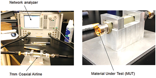
Figure 3 The solid cylinders are machined as sleeves to specific dimensions that fit inside the 7 mm coaxial airline standard and measured in the test setup.
Voxel8 specifies their proprietary silver ink with a volume resistivity below 5.0×10⁻⁷ Ω-m. Even lower values have been verified by printing traces, letting them dry for eight hours, and measuring their cross sectional area with a laser profilometer, and their resistance with a 4-point probe. To verify these direct conductivity measurements using a printed RF part, a 50 Ω microstrip line was modeled using CST’s computational electromagnetic tool using the measured dielectric constant for the substrate material.
Voxel8 printed two 4" microstrip circuit (plastic, substrate and conductive trace) samples and MITRE added coaxial connectors and an aluminum plate to hold the connectors. Voxel8’s silver ink was dispensed from a syringe as an electrically conductive adhesive to attach the connector to the microstrip trace instead of using conventional solder. Figure 7 shows that the measured results are in good agreement with simulation.

Figure 4 Electrical properties for one of the extruded PLA samples using Voxel8 printer - grey colored sample.
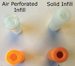
Figure 5 Comparison of test samples made by adding air perforation to the material and normal samples.
In the 4" sample, the 3D printed microstrip has approximately 1 dB more loss at 12 GHz than that in a similar microstrip line model using a traditional PCB substrate with a ½ oz. electrodeposited (ED) copper trace (see Figure 7). The additional loss is believed to be due to the surface roughness (19 microns) of the 3D printed silver trace, which is much higher than typical ED copper (0.5 micron). After re-simulating the 3D printed microstrip line using a lower surface roughness (0.5 micron) and same measured resistivity of Voxel8’s silver ink, the difference in the simulated losses was reduced to less than 0.5 dB at 12 GHz.
Wi-Fi Antenna Measurement
A simple printed monopole Wi-Fi antenna was manufactured and measured. Three different samples were made using three different 3D printers, at three different times in order to test the repeatability of the process. Again, the connection to the coaxial cable was made by a dot of Voxel8’s silver ink dispensed from a syringe. The measured VSWRs are found to be consistent with simulation and the results are repeatable as shown in Figure 8. The radiation patterns were also measured at MITRE’s antenna chamber. A symmetric omnidirectional beam was seen in the measurements, which agrees with the simulation as shown in Figure 9. Lastly, the antenna was cycled through temperature extremes from -40° to 60°C, and didn’t show significant impact on measured patterns or VSWR after thermal cycling.
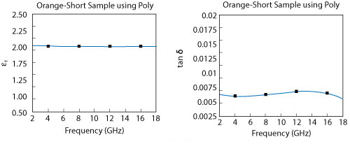
Figure 6 The measured material properties of the partially infilled PLA.
After subjecting the antenna to extreme external temperatures, the effects of electrically induced temperature from high power transmission were measured. MITRE powered a 3D printed antenna with 30 W for five minutes without adverse effect on electrical performance or structural integrity.
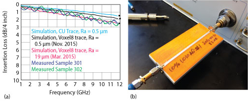
Figure 7 Validating Voxel8’s conductivity by comparing the measured insertion loss to simulation using the electrical properties of Voxel8 materials.
3D Printing - Complicated Structure
Additive manufacturing has opened the design space to realize increased design sophistication and manufacturing agility that leads to increased access and operational effectiveness. MITRE is currently exploring the potential for a high performance 3D printed metamaterial structure and a 3D printed wideband phased array design.
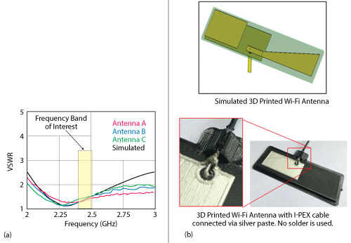
Figure 8 VSWRs of three Wi-Fi antennas made using three different 3D printers, at three different times including photos.
3D Printed Metamaterial Structure
Metamaterials are composed of an assembly of subwavelength structures that exhibit bulk properties not found in nature. One such property is negative index of refraction. Many of the metamaterial designs in the literature require the incident electric field to be polarized in a particular direction in order for the extraordinary metamaterial properties to exist.5,6 MITRE is working on a biaxial metamaterial that supports fields with multiple incident polarizations.
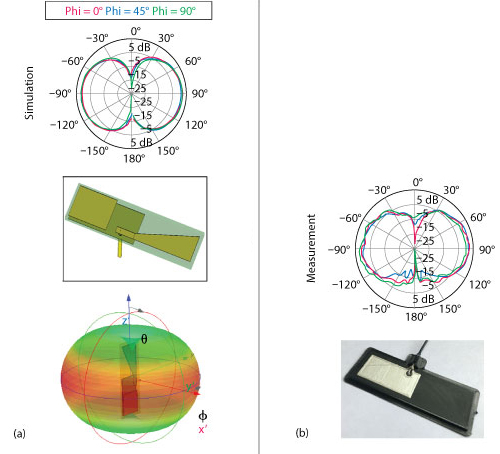
Figure 9 Radiation patterns at 2.45 GHz showing good agreement between simulation (a) and measurement (b).
An early negative index of refraction metamaterial was composed of a lattice of split ring resonators (SRR) combined with rods.5 The split ring resonators create a negative permeability and the rods created a negative permittivity. When the structures were combined, a negative index of refraction was achieved. However, this property only exists if the incident electric field is aligned with the rods and the magnetic field goes through the split ring resonators as shown in Figure 10a. An alternative structure called the S-shaped split ring resonator (S-SRR), shown in Figure 10b, was proposed in reference 6 and exhibits similar properties to the combined SRR and rods. Again, the electric field must be aligned in a particular direction, i.e., along the longer axis of the S-SRR, and the magnetic field must go through the loops.
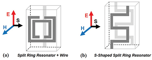
Figure 10 A negative index of refraction metamaterial unit cell composed of a split ring resonator combined with a rod (a) and an S-shaped split ring resonator unit cell (b).
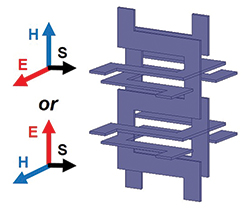
Figure 11 MITRE’s biaxial metamaterial unit cell with intersections that can be easily 3D printed, but would be difficult to manufacture otherwise.
MITRE’s biaxial metamaterial is based on the S-SRR. The interesting feature in this design is an orthogonal and intersecting copy of the unit cell. This metamaterial is composed of intersecting three dimensional lattices that are relatively easy to 3D print, but would be very difficult, if not impossible, to make with conventional methods. The orthogonal structures allow the metamaterial to keep its properties, like negative index of refraction, for multiple electric field polarizations, whereas the original structure only works when the electric field is aligned in a particular direction. When using a metamaterial on a mobile platform where the direction or polarization of the incident fields is not known, it is easy to see the advantages of this modified metamaterial. Figure 11 shows a model of the biaxial S-SRR unit cell structure. The metamaterial properties are the same when the incident electric field is vertically or horizontally polarized.
The biaxial S-SRR was simulated using periodic boundary conditions and Floquet ports in HFSS. The passband occurs from approximately 5 to 5.5 GHz, as seen from the simulated S-parameters in Figure 12a. The reflection and transmission coefficients were used to calculate the effective index of refraction using the Nicolson-Ross-Weir method.7 Figure 12b shows that the index of refraction is negative in the passband of the metamaterial, with a value of approximately -0.3 at 5 GHz. The passband and the value of the index of refraction can be controlled by varying the metamaterial dimensions.
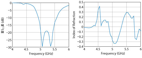
Figure 12 Simulated reflection coefficient of the biaxial metamaterial (a) and calculated index of refraction of the metamaterial with a negative value within the passband (b).
Figure 13 shows a small test coupon of the biaxial metamaterial created using a Voxel 8 multi-material 3D printer. Several coupons will be manufactured to measure the reflection coefficients when they are mounted inside a waveguide fixture.
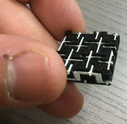
Figure 13 A small test coupon of MITRE’s biaxial metamaterial created with a Voxel8 multi-material 3D printer.
3D Printed Phased Array
MITRE developed a wideband phased array concept that has a complex design. It is based on a printed circuit board (PCB) design that was not physically realizable. The design resembles an egg-crate construction with contiguous electrical connection (interdigitiated fingers) that is embedded within the orthogonal board interface as illustrated in Figure 14.
Multi-material additive manufacturing is thought to be the only practical way to realize this design. Voxel8 printed a sample of the cross in the middle of the array. The CT-scan shows the details of all of the fingers. The details of the design will be discussed in a future publication. Currently we are building a finite size array to be measured at MITRE.
Conclusion
Recent advances in multi-material additive manufacturing have enabled complex RF structures to be realized. The characterization of the materials used in additive manufacturing processes has been shown to be of utmost importance in designing and accurately predicting performance of these structures. Understanding the RF properties of the materials through rigorous characterization has led to the development of novel prototype structures, like the biaxial metamaterial and phased array antenna with interdigitated fingers. Future efforts will focus on utilizing advanced additive manufacturing methods to realize even smaller RF structures for higher frequency applications. As the materials and methods of multi-material additive manufacturing improve, RF structures that could previously only be imagined will be easily built for low cost implementation of advanced technologies.

Figure 14 3D printed phased array design with complex features.
Acknowledgments
The authors would like to thank Prof. Jennifer Lewis, Karl Willis, Jack Minardi, Kyle Dumont and Daniel Thompson from Voxel8 for their technical discussions and collaboration in this project. They would also like to thank Cecelia Franzini and Erin Jaffke of the MITRE Corporation for their contributions to the effort.
Disclaimer
In support of our government sponsors, The MITRE Corporation evaluates technology and collaborates with industry and academia as appropriate. The article reflects the results of such testing and/or collaboration and is not intended to be an endorsement of any technology or product.
References
- Voxel8 website, www.voxel8.co/.
- Keysight Technologies 85051B 7 mm Verification Kit, www.keysight.com/.
- Keysight 85071E Materials Measurement Software, www.keysight.com/.
- Voxel8’s materials, www.voxel8.co/materials/.
- D.R. Smith, W.J. Padilla, D.C. Vier, S.C. Nemat-Nasser and S. Schultz, “Composite Medium with Simultaneously Negative Permeability and Permittivity,” Phys. Rev. Lett., Vol. 84, No. 18, May 2000.
- H. Chen, L. Ran, J. Huangfu, X. Zhang and K. Chen, “Left-Handed Materials Composed of Only S-Shaped Resonators,” Phys. Rev. E, Vol. 70, 2004.
- A.M. Nicolson and G.F. Ross, “Measurement of the Intrinsic Properties of Materials by Time Domain Techniques,” IEEE Trans. Intrum. Meas., Vol. IM-19, pp. 377–382, Nov. 1970.