
A super linearity high power amplifier uses the feedforward technique. A key element of this technique, an adjustable vector modulator, is made of passive devices. The advantage of passive devices, compared with active devices, is that they do not distort high power signals. In order to improve cancellation of intermodulation products, this adjustable vector modulator has high resolution as well. A 50.4 dBm output power amplifier with -62 dBc third-order intermodulation distortion is demonstrated.
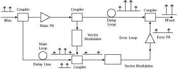
Figure 1 Feedforward system block diagram.
The VHF power amplifier is widely used in wireless applications and is a critical transmitter component. Its purpose is to produce a high signal output for proper transmitter operation. This may be achieved, however, at the expense of linearity. Normally, the third-order intermodulation distortion of a Class A amplifier at 1 dB compression is no better than -20 dBc. This is far above the requirement of many systems, where third-order intermodulation distortion must be -50 dBc with greater than 50 dBm output power.
There are three main methods to linearize an amplifier: feedback, predistortion and feedforward.1 The feedforward technique is widely used because it can achieve the best linearization performance,1-3 but low efficiency is a major drawback. Appropriate power-retreat has often been used to provide suitable third-order intermodulation distortion before linearization is employed. In our system, the main power amplifier is retreated to a third-order intermodulation distortion of -39 dBc with 52.5 dBm output power. This is good performance, but is still not sufficient. The adaptive feedforward technique can be used to meet today’s system requirements in the presence of environmental variations,4 but it is rarely used in high power systems because it uses an electronically adjustable vector modulator employing active devices. When RF power is high, active devices introduce distortion. In our approach, however, an adjustable vector modulator composed of passive devices provides high resolution to realize excellent cancellation of third-order intermodulation products. With the exception of the main amplifier and the error amplifier, the devices in this system are passive. Experimental results show that third-order intermodulation distortion is reduced from -39 dBc for original amplifier with an output power of 52.5 dBm to -62 dBc for the linearized amplifier with an output power of 50.4 dBm.
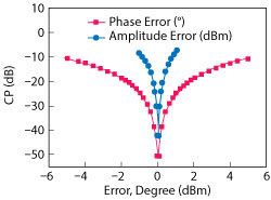
Figure 2 Cancellation of two equal-amplitude, anti-phase signals as a function of phase or amplitude error.
Cancellation Performance of Signals
Since the feedforward linearizer is designed to eliminate third-order intermodulation distortion through cancellation, the cancellation of two signals is analyzed (see Figure 1). Assuming that the two signals are sinusoidal, the greatest cancellation occurs when their amplitudes are equal and their phases are opposite. The relationship between cancellation performance versus amplitude and phase error is5
where CP is the cancellation performance, Verr is the voltage amplitude error, Vm is the voltage amplitude of the signals and θerr is the phase error. It is apparent that CP is more sensitive to amplitude error and decreases with the rise of signal power.
Simulation (see Figure 2) shows the effects of amplitude and phase mismatch on the CP of two signals. The power of each signal is 10 dBm with a phase difference of 180 degrees in order to simulate the third-order intermodulation distortion of the main amplifier. The intermodulation signals can be suppressed by more than 30 dB only when the phase error is less than 0.5 degrees and the amplitude error is less than 0.08 dBm. This is hard to achieve in practice. To ensure that the CP is small, high resolution of the vector modulator is necessary.
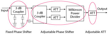
Figure 3 Vector modulator block diagram.
For a dual-tone signal, CP is also affected by the group delay of each delay line, as shown in Equation 2.5

where f0 is the center frequency, λ0 is the wavelength at the center frequency and Lerr is the length difference between the delay lines. CP is less sensitive to Lerr as compared with α and θerr. Lerr can be decreased by adjusting the lengths of the delay lines.
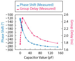
Figure 4 Vector modulator phase shift and group delay as a function of capacitor value.
Feedforward System Design
As shown in Figure 1, this feedforward system is composed of a main loop and error loop. The main loop includes the main amplifier, couplers, delay line and vector modulator. The function of main loop is to suppress the signal in order to extract the third-order intermodulation distortion for input to the error loop. The error loop is composed of the error amplifier, couplers, delay line and vector modulator. Its function is to eliminate third-order intermodulation distortion of the main amplifier output using the output of main loop. To realize a super linearity, both loops must have excellent cancellation performance.
In order to minimize insertion loss and preserve overall efficiency, the main path consists only of couplers, the main amplifier and delay line. Efficiency can be expressed as

where η' is the overall system efficiency, η is the overall efficiency of the main and error amplifiers, OPm and OPe are the amplifier output powers, TLm is the transmission loss of main path and Pback is the retreated power of the error amplifier. Because OPm is much larger than OPe, η' is more sensitive to TLm. This implies that TLm must be minimized.

Figure 5 Output spectrum of the main amplifier vs. output power of the main loop.
Figure 3 is a block diagram of the vector modulator. It consists of a fixed phase shifter, an adjustable phase shifter and an adjustable attenuator. The fixed phase shifter is composed of a 3 dB quadrature coupler and two equivalent capacitors. Figure 4 shows test results for the fixed phase shifter. Capacitor values can be adjusted to change the phase shift and group delay. The adjustable phase shifter is composed of a 3 dB quadrature coupler, two adjustable attenuators and a Wilkinson power divider. The principle is illustrated by
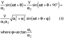
α1, α2 are the voltage attenuation values of the two paths and φ is the phase shift of the vector modulator.
The input is divided into two equal amplitude signals with 90 degree phase difference by the 3 dB quadrature coupler. The two signals pass through attenuators and are combined in the Wilkinson power divider. The phase shift is determined by α1 and α2 controlled by the attenuators. The ideal phase shift of the vector modulator is 90 degrees. Over the range of attenuation, the vector modulator can achieve only about 75 degrees phase shift, however; so a fixed phase shifter is added in front of the vector modulator to provide a suitable phase shift and group delay. Furthermore, the vector modulator produces some degree of attenuation determined by α1 and α2. An adjustable attenuator is added at the output to control overall attenuation. Adjusting the length of delay lines and the capacitor values equalizes the group delays. The phase shift at the center frequency is adjusted by the attenuation in each path. To provide equal dual-tone signal amplitudes, an LC network is placed before main amplifier to compensate for an uneven gain curve.
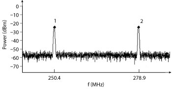
Figure 6 Output spectrum of the error loop.
Amplitude and phase resolution of the vector modulator is determined by the adjustable attenuator at the output. In this system, when the CP is about -30 dB, less than a 0.01 dB change in amplitude and a 0.06 degree change in phase, respectively, will lead to a 1 dB change of CP. The adjustable attenuator used is manually adjustable and its resolution is as high as 0.01 dB, corresponding to a phase resolution for the vector modulator of less than 0.06 degree.
Test Results
Analysis shows that, to meet system requirements, the output power of error amplifier should be about 30 dBm. A power amplifier with a 1 dB compression point of about 47 dBm and gain greater than 65 dB is chosen to provide adequate linearity. At an output power of 30 dBm, third-order intermodulation distortion is less than -45 dBc. The main amplifier center frequency is 264.6 MHz with 10 MHz bandwidth. The power gain is about 50 dB with 1 dB gain flatness. The input is a dual-tone signal at 259.9 MHz and 269.4 MHz, respectively, each at 3 dBm.
Figure 5 shows the output spectrum of the main amplifier versus the output power of the main loop, indicating that cancellation may be as high as 35 dB. Cancellation of feedforward system, however, is determined by the error loop, which is tested individually.
The dual-toned test signal for the error loop is 10 dBm (each tone) at 250.4 MHz and 278.9 MHz, respectively. Figure 6 is the output spectrum of the error loop. Values at the marker points are -22.68 dBm (MKR1) and -22.59 dBm (MKR2), indicating that the input signal can be suppressed more than 32 dB in error loop.

Figure 7 System output spectrum with the error amplifier disconnected.
Finally, the entire feedforward system is tested, with a 58 dB attenuator at the output to protect the spectrum analyzer. Figure 7 is the output spectrum of the entire system with the error amplifier disconnected. The four markers are at -10.28 dBm (MKR1), -10.14 dBm (MKR2), -45.31 dBm (MKR3) and -51.75 dBm (MKR4). The main amplifier is driven to an output power of 52.5 dBm and the left and right third-order intermodulation products are -38.7 dBc and -41.1 dBc respectively. The transmission loss of the path between the main amplifier output and the system output connector is approximately 2 dB, including delay line and coupler losses.
Figure 8 is the output spectrum of system with the error amplifier connected. The markers are at -10.65 dBm (MKR1), -10.59 dBm (MKR2), -72.53 dBm (MKR3) and -72.36 dBm (MKR4). It shows the third-order intermodulation distortion of main amplifier suppressed from -48 dBm to -72.3 dBm. Fifth-order intermodulation distortion is also suppressed to the background noise. Third-order intermodulation distortion of the system is approximately -62 dBc. The cancellation is 24 dB on the left and 21 dB on the right. From Figures 7 and 8, the main signals are suppressed about 0.4 dB due to residual signals from the main loop.
Conclusion
A super linearity high power feedforward amplifier is realized based on the feedforward technique. A key element of feedforward system, a high resolution adjustable passive vector modulator is designed in order to fully suppress third-order intermodulation products. Third-order intermodulation distortion of the linearized amplifier is -62 dBc at an output power of 50.4 dBm. High output power with low third-order intermodulation distortion makes the system attractive in transmitters for today’s wireless applications. Moreover, the adjustability of the vector modulator makes the system useful for other frequency bands and bandwidths.
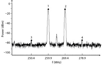
Figure 8 System output spectrum with the error amplifier connected.
Acknowledgment
This work was supported by the National Natural Science Foundation of China, under grant No. 61001012.
References
- A. Mohammadi and F.M. Ghannouchi, “RF Transceiver Design for MIMO Wireless Communications,” Springer-Verlag Berlin Heidelberg, 2012, 1st edition.
- M. Faulkner, “An Automatic Phase Adjustment Scheme for RF and Cartesian Feedback Linearizers,” IEEE Transactions on Vehicular Technology, Vol. 49, No. 3, May 2000, pp. 956–964.
- J. N. Swaminathan and P. Kumar, “Design and Linearization of Solid State Power Amplifier Using Pre-Distortion Technique,” International Conference on Computer Communication and Informatics (ICCCI), January 2013, pp. 4–6.
- J.K. Cavers, “Adaptation Behavior of a Feedforward Amplifier Linearizer,” IEEE Transactions on Vehicular Technology, Vol. 44, No. 1, February 1995, pp. 31–40.
- S.G. Kang, I.K. Lee and K.S. Yoo, “Analysis and Design of Feed-Forward Power Amplifier,” IEEE International Microwave Symposium Conference Digest, Vol. 3, June 1997, pp. 1519–1522.