
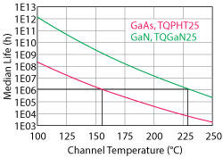
Figure 1 Reliability comparison of Qorvo GaN and GaAs PHEMT processes.
Editor’s Note: Because of its high power density, GaN is widely recognized as providing a step-function increase in the capability of solid-state power amplifiers. Arguably not as well known is the impact GaN is having at the system level, particularly military systems. While logical to assume GaN enables evolutionary improvements, in some cases the system would not be possible without GaN. The Space Fence radar is one example, described in this article by Lockheed Martin.
GaN 101
GaN is a compound semiconductor using III/V group elements that represents a leap ahead of existing GaAs technologies for many RF applications. GaN high electron mobility transistors (HEMT) are constructed using very similar fabrication techniques as GaAs RF devices but provide significant advantages.
The reason for the leap in technology GaN has over GaAs results from significantly higher operating RF power density and higher reliability. The secondary benefits built on these first two are: smaller chips for a given output power; smaller modules; higher overall efficiency due to lower combining losses; lower module assembly cost; higher power handling survivability and higher impedance for large devices, making for easier impedance matching.
The inherent advantage of GaN over GaAs is due to basic physics of the devices and materials. GaN is referred to as a wide bandgap semiconductor because of the wider energy gap between the valence and conduction bands, compared to conventional semiconductors. The wider energy gap (3.4 eV for GaN compared to 1.42 eV for GaAs) allows higher electric field strengths and higher breakdown fields, which translate into higher operating voltages.1
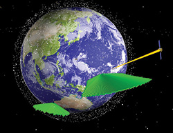
Figure 2 Space Fence comprises two radars, one located near the equator at Kwajalein Atoll and an optional second site in Western Australia.
Another advantageous characteristic of GaN is electron drift velocity, which in GaN increases with higher field strength, while it decreases with higher field strength in GaAs. Another way of describing it is that the low field drift velocity of GaAs is superior to GaN, but the high field drift velocity of GaN is far superior to GaAs. The peak in this characteristic (electron drift velocity vs. field strength) is the saturation velocity. In GaN it is 2.46 × 107 cm/s, while GaAs is 1.8 × 10⁷. However, at high fields where GaN is 2.46 × 10⁷, GaAs electron drift velocity is under 1 × 107.1 Since electron drift velocity is related to current density, it basically means that at high voltage, GaN is also capable of high current, whereas GaAs is not. Also, since power is a function of voltage and current, the wide energy gap and high drift velocity make for ideal high power devices. For these reasons, GaAs will never outperform GaN for high power applications; however GaAs should retain its applicability in low voltage and low power applications.
A third important aspect of GaN technology, especially for power devices, is the substrate material. Since GaN substrates were not very advanced and were thermally inferior, silicon carbide (SiC) emerged as the best substrate material for GaN RF power devices. The thermal conductivity of SiC is superior to other substrates, such as silicon or sapphire, and allows the high power potential of GaN to be realized. The thermal conductivity of SiC is approximately 10× better than GaAs. These advantages allow operation of systems and sensors that would not have been possible with GaAs semiconductors. For example, new systems have steep requirements for both performance and operational availability. GaN enables sensors to operate with longer reliability and be driven harder (i.e., longer pulse width per duty cycle), based on the inherent higher power density properties.
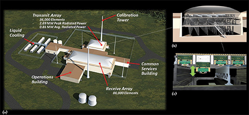
Figure 3 Space Fence radar site (a) cutaway of the transmit array (b) and cross-section of the “radar-on-a-board” transmit LRUs (c).
Assessing reliability, GaN devices can operate at a much higher channel temperature than GaAs for equivalent reliability; at equivalent channel temperatures, GaN achieves much higher reliability. Comparing the reliability of Qorvo’s GaN and GaAs technologies (see Figure 1), at Tc = 150°C the median life of GaN is 1 × 10⁹ hours vs. 1 × 10⁶ hours for GaAs. At 1 × 10⁶ hour median life, GaN can operate 75ºC hotter than GaAs (i.e., 225°C for GaN vs. 150°C for GaAs).2
Overall, GaN can lead to smaller, cheaper, more efficient and higher power RF modules. For example, a single GaN MMIC high power amplifier (HPA) can replace a pair of GaAs HPAs which need a power combiner/divider, extra supporting components and additional assembly. Efficiency is gained not only at the MMIC level, where on-chip combining losses are reduced, but also at the module level, where combining losses are eliminated when two or more GaAs HPAs need to be combined.
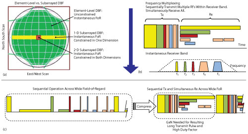
Figure 4 Digitizing at the element, instead of combining multiple elements into subarrayed receivers, enables beams to be formed anywhere in the array FoR (a). Multiple frequency channels, each for a different radar function, can be received at the same time by beams on the receive array, allowing many functions to be performed simultaneously (b). GaN is the only technology that supports the “machine gun” transmit sequence, with long pulses and high duty factor (c).
Use of GaN HPAs in solid-state phased array radar provide numerous benefits. As described, GaN supports higher output power, higher transmit duty factor and longer pulse lengths than previous technologies, such as GaAs and Si BJT. These allow smaller aperture sizes and reduce overall system acquisition costs. Since GaN operates at higher efficiency, operational costs are also reduced, as less prime power is consumed and less heat is dissipated, reducing the need for active cooling. An example of this would be an existing radar which utilizes a solid-state semiconductor such as GaAs. An equally sized radar employing GaN would benefit from a significant increase in radar range with a slight increase in prime power. Conversely, for the same prime power, the power density of GaN could significantly reduce the radar aperture. This has first order effects of reducing acquisition costs, including both front-end and back-end electronics. Lastly, GaN has higher reliability than previous technologies. Higher reliability reduces operational costs through reduced maintenance and spare parts.
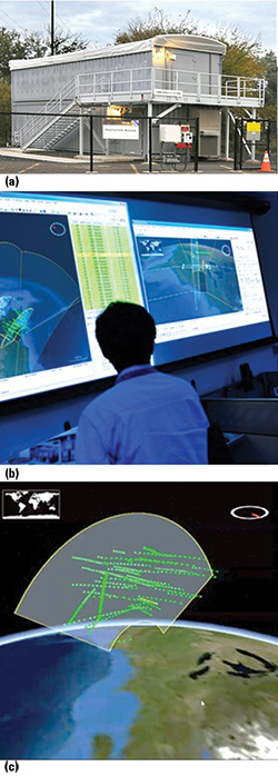
Figure 5 Space Fence prototype: antenna building (a) mission operations center (b) and critical design review (CDR) demonstration.
SPACE FENCE RADAR
Space Fence is a ground-based system of S-Band radars designed to greatly enhance the U.S. Air Force Space Surveillance Network. Space Fence provides unprecedented sensitivity, coverage and tracking accuracy and contributes to key space mission threads, with the ability to detect, track and catalog small objects in low Earth orbit (LEO), medium Earth orbit (MEO) and geosynchronous orbit (GEO). Space Fence’s capabilities of detecting, tracking and cataloging hundreds of thousands of satellites and debris in orbit around the earth will revolutionize space situational awareness.3
Space Fence includes up to two minimally manned radar sites (see Figure 2). The first radar site is under construction on Kwajalein Atoll in the Pacific Ocean near the equator and is expected to become operational in late 2018. The second site, currently an unfunded contract option, is located in Western Australia. The sensor sites provide assured coverage for objects in LEO and are integrated through an operations center located in Huntsville, Ala.
The initial Kwajalein radar will provide a persistent surveillance “fence” comprised of thousands of radar beams covering LEO altitudes. As the Earth rotates, this fence sweeps the space around the Earth, providing assured coverage to detect satellites and orbital debris. To form high quality orbital estimates, objects that cross the fence are tracked over long arcs with dedicated beams. Space Fence can also be tasked to search for higher altitude objects in MEO and GEO. The optional second site will complement the first site’s LEO coverage and also provide tasking capability to MEO and GEO.3
As shown in Figure 3a, each radar site features a design with closely spaced but separate transmit and receive phased array antennas, prime power and liquid cooling. The transmit array building houses a 36,000 element transmit phased array antenna beneath an air supported low loss Kevlar environmental radome. The receive building supports an 86,000 element array, also under a low loss Kevlar radome. Both arrays are provided power and cooling through the common services building. Radar data processing and control of the apertures is performed off-array in commercial off-the-shelf (COTS) processing equipment located within the operations building. Both transmit and receive arrays are automatically calibrated with horns that are mounted on calibration towers and can transmit or receive test signals. The extremely large phased arrays are optimized for high availability and low lifetime support costs and use GaN HPAs for transmit amplification, providing unprecedented sensitivity to detect small objects. On receive, digital beam forming (DBF) at the element level permits thousands of simultaneous beams instantaneously in any direction. This enables the system to provide persistent LEO surveillance coverage while simultaneously tracking hundreds of objects, performing cued search tasks in other surveillance regimes (including MEO and GEO) and supporting user-defined flexible surveillance volumes. Transmit and receive arrays are oriented to face straight up and are designed integrally with the building (see the transmit array cutaway in Figure 3b). A scalable facility structure supports liquid cooled cold plates, which house the radar electronics. Radiator tiles are mounted on the top of the cold plates while “radar-on-a-board” digital transmit and receive line replaceable units (LRU) are mounted on the sides (see Figure 3c). Each transmit LRU incorporates digital waveform generation, up-conversion to S-Band and high power GaN amplification for eight transmit radiating elements. Mounting the LRUs on the sides of the cold plates provides the GaN HPAs with a direct and efficient thermal path. To provide high system availability, the LRUs are serviceable from beneath the array and can be removed and replaced in less than 1½ minutes while the array is operating.
GaN high power amplification was one of the critical enabling technologies for the Space Fence solution. Relative to other technologies, the high output power of GaN reduces the number of transmit elements to achieve the required sensitivity for the target size, which reduces overall acquisition cost. GaN’s high efficiency also reduces power consumption and heat dissipated, which reduces operational costs for the sensor site. In order to effectively support the LEO orbital regime (and tasking up to GEO) and get sufficient energy back for detection, transmit pulse lengths need to be long. Previous technologies, such as GaAs or Si BJT didn’t support these pulse lengths at the required output power.
The long pulse capability of GaN in the transmit array also enables extremely efficient timeline utilization of the radar when combined with element level DBF in the receive array. Space Fence has a receiver connected to each array element within the receive array to digitize the returned signals. Unlike subarrayed antennas, which combine multiple elements in microwave electronics prior to digitizing to reduce the number of receivers, the beams in an element level DBF system can be simultaneously placed anywhere in the field-of-regard (FoR) of the array. Subarrayed approaches limit the digitally formed beams to constrained volumes and require changing analog phase shifters to move the volume from one radar event to the next (see Figure 4a). Space Fence is able to use its flexibility along with frequency multiplexed functions within the receiver band to form thousands of beams simultaneously (see Figure 4b). This allows many functions that would have been performed sequentially to be performed simultaneously, reducing the Space Fence array sizes along with the associated acquisition cost and operating costs. Use of GaN HPAs are needed to support the resulting concatenated “machine gun” like transmit sequence, which is longer and transmit higher duty factor than supported by other technologies (see Figure 4c).
At the start of concept development for Space Fence in 2007, Lockheed Martin leveraged an existing Independent Research and Development (IRAD) project that was maturing GaN for use in radar applications. Over the course of the Space Fence development, GaN was optimized to the Space Fence application for additional efficiency and reduced operational costs. Lockheed Martin also embraced an open foundry concept and worked with two suppliers to develop GaN for Space Fence. Space Fence transmit LRUs have been successfully tested with GaN modules from both of these companies. Use of multiple suppliers reduced program risk and provided competition to reduce acquisition costs.
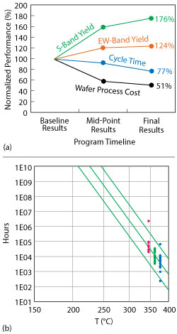
Figure 6 Wolfspeed DPA Title III performance improvement (a) and reliability (b).
With the large Space Fence arrays and number of GaN devices, high reliability is necessary to keep maintenance costs down. To ensure mature technology, Lockheed Martin tested the Space Fence GaN amplifiers at the module, at the transmit LRU and at the array. After years of extensive testing (more than 5,000 hours of life testing, including accelerated life testing), the technology has proven to be extremely robust, showing a high reliability confidence level which supports the rigorous operational availability of the mission.
Since 2011, Lockheed Martin has had an operational end-to-end system prototype employing all its critical technologies, including GaN and element level DBF, in scaled-down arrays (see Figure 5). Prototype system data was used by the U.S. Air Force in a technology readiness assessment in 2015, resulting in a Technology Readiness Level (TRL) 7 and Manufacturing Readiness Level (MRL) 7. In January 2016, an Integration Test Bed (ITB) using final production hardware was commissioned in Moorestown, N. J. The ITB supports hardware/software integration, maintenance training and verification testing; it will provide remote support to the integration of Sensor Site 1 on Kwajalein Atoll.
OPEN FOUNDRY MODEL
The development of GaN with ever increasing government funding has been occurring since the 1970s.4 Since the early 2000s, both the Department of Defense and commercial foundries have considerably increased this funding. One example is the DARPA Wide Bandgap program which funded various semiconductor foundries to mature the technology, investing approximately $150 million. This program followed the successful initiatives of the 1980s and 1990s to fund GaAs, such as DARPA’s MIMIC and MAFET programs. Among the key parameters and facets of the technology development were the physics of the devices, to understand and unleash the potential of the superior physical properties of the semiconductors, and the development of accurate models.
The completion of the DARPA Wide Bandgap program in 2011 led to an additional program funded through the Defense Production Act (DPA) Title III program office. The mission of the DPA Title III program is to “create assured, affordable and commercially viable production capabilities and capacities for items essential for national defense.” The main focus of the GaN Title III program was to improve the manufacturability of GaN, essentially to increase the MRL to level 8. The program was structured as three phases: 1) baseline manufacturing readiness, 2) improvement and refinement of processes and 3) final manufacturing readiness assessment.
Wolfspeed was able to substantially increase their yield over the three phases, while simultaneously reducing cycle time and wafer processing costs (see Figure 6).5 Over the three phases, yield increased 76 percent for S-Band devices, cycle time reduced 23 percent and wafer costs decreased 49 percent. Reliability of 1 × 10⁷ hours was demonstrated at a channel temperature of approximately 275°C. Through manufacturing process refinement and building significant robust wafer lots, Wolfspeed reached MRL 8 in 2014, i.e., demonstrated pilot line capability and ready to begin low rate initial production (LRIP). One of the other major commercial foundries, Qorvo (formerly TriQuint) was the only funded foundry that achieved MRL 9 in 2014, i.e., demonstrated LRIP and capability in place to begin full rate production (FRP).
GaN has been inserted into several Lockheed Martin and other DoD contractor systems and has achieved TRLs through level 9. Space Fence has achieved TRL 7. Since the completion of both the DARPA Wide Bandgap and DPA Title III programs, GaN has been following a Si CMOS trajectory, in terms of applications and utilization in commercial markets.6 GaN has found its way into base stations, medical equipment and even residential/commercial lighting available at local hardware stores (see Figure 7).
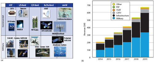
Figure 7 Commercial and military products using GaN (a) and projected GaN market growth (b). Commercial pull for GaN will be more than 2x military applications by 2019.6
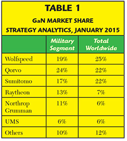
Lockheed Martin employs an open foundry model (LM OpenGaN), which leverages the commercial market for the best technology at the most competitive cost. The cost of owning and running a foundry year after year can be significant. Given the growth projections for semiconductors, in general, it makes more sense to allow high commercial volumes to mature the technology process and drive costs down.7 A study conducted by Strategy Analytics6 (see Table 1), identified Qorvo and Wolfspeed as GaN leaders, with no other domestic suppliers close to providing equivalent volume. In the semiconductor industry, volume production lends itself to higher maturity, stable processes and lower costs.
Lockheed Martin adopted an open foundry model to address the Department of Defense’s official memorandum on Better Buying Power 3.0 and the “3rd Offset,” with the goal of increasing the capability and rapid technology development required by the warfighter.8 It is not economical to have any particular foundry develop various semiconductor processes, not just III/IV (i.e., GaAs, GaN, InP) but also SiGe and CMOS.
GaN has had significant investment over the past 10 years and is proven to be field ready, reliable and cost competitive with existing technologies (e.g., GaAs). The system benefits enable enhanced capabilities for backfit military systems and are required for the performance of future systems. The Space Fence program would not have been possible without GaN nor as successful without the affordability enabled by the LM Open GaN foundry model.
THE FUTURE
The next generation of GaN development is focused around increasing capability by pushing into higher operating frequencies, improving thermal performance and enabling chip-scale integration of GaN with other IC technologies. Developments of 150 nm and 90 nm process nodes will extend ft to 60 and 100 GHz, respectively.
While DBF systems such as Space Fence represent a significant capability upgrade, the challenges from the increased IC design complexity in the areas of size, weight and power (SWAP), bandwidth and latency performance must be overcome. To address this, programs such as DARPA’s Diverse Accessible Heterogeneous Integration (DAHI) program are focused on developing chip-scale integration of GaN with high density Si CMOS, as well as other technologies such as InP and MEMS. These resulting capabilities will enable the wider proliferation of the high performance mixed-signal integration solutions required to develop the capabilities to further advance state-of-the-art sensor systems.
While GaN is capable of generating extremely high RF power densities, thermal management remains a significant challenge, especially at higher frequencies where thermal density is most extreme. On the DARPA IceCool program, Lockheed Martin has made tremendous gains in unlocking the ultimate potential of millimeter wave GaN by developing a micro-fluidically cooled HPA with a 3×reduction in thermal resistance compared to conventional thermal management solutions. This IceCool solution enables an 8.3 dB increase in output power for the same device, while simultaneously reducing operating temperature by increasing power-added efficiency between 2.5× and 3.5×.9 Overall, these advancements will further extend the true potential of GaN and its ability to realize tremendous capability upgrades for a wide variety of systems.
ACKnowledgment
The authors would like to acknowledge and thank the Space Fence and ICECool sponsors (AFLCMC, DARPA and AFRL) and partners for their financial and technical support.
References
- Liou Schwierz, “Modern Microwave Transistors,” Wiley, 2003.
- R. Hall, “GaN at Qorvo” Presentation, August 2015.
- Joseph A. Haimerl and Gregory P. Fonder, “Space Fence System Overview,” Advanced Maui Optical and Space Surveillance Technologies Conference Proceedings, September 2015.
- M. Yoder, “Gallium Nitride Past, Present, and Future,” IEEE/Cornell Conference on Advanced Concepts, 1997.
- Ryan Fury, Scott T. Sheppard, Jeffrey B. Barner, Bill Pribble, Jeremy Fisher, Donald A. Gajewski, Fabian Radulescu, Helmut Hagleitner, Dan Namishia, Zoltan Ring, Jennifer Gao, Sangmin Lee, Brian Fetzer, Rick McFarland, Jim Milligan and John Palmour, “GaN on SiC MMIC Production for S-Band and EW-Band Applications,” CS ManTech Conference, May 13–16, 2013, New Orleans, La.
- Eric Higham, Strategy Analytics, “An Overview of GaN RF Device Market,” GaN Roundtable Session, August 26, 2015.
- Justin Gallagher, “The Commercialization of GaN,” Defense Manufacturing Conference Proceedings, November 2015.
- Under Secretary of Defense, “Implementation Directive for Better Buying Power 3.0 – Achieving Dominant Capabilities through Technical Excellence and Innovation,” Memorandum, 2015 http://bbp.dau.mil/docs/BBP3.0ImplementationGuidanceMemorandumforRelease.pdf.
- J. Ditri, R. Cadotte, D. Fetterolf and M. McNulty, “Impact of Microfluidic Cooling on High Power Amplifier RF Performance,” Proceedings of the 15thIntersociety Conference on Thermal and Thermomechanical Phenomena in Electronic Systems (ITHERM 2016), Las Vegas, Nev., 2016.