
A fully printable 3D stacked chipless RFID tag on a 50 µm thin polyimide film consists of multi-layer cross-polarized dipole resonators that overlap. Data encoding is performed in a multiresonating circuit comprised of multiple stopband resonators. The resonators are screen printed with a silver based conductive paste. The chipless RFID tag is designed specifically for security applications suitable for mass deployment (trillions) of low cost items.
Research efforts have been devoted to developing RFID tags with no ASICs in an effort to lower the price of the RFID system.1 Chipless RFID tags have been designed and reported by researchers around the world. Encoding data without an IC is accomplished mainly by encoding schemes based on either time domain reflectometry (TDR) or spectral signatures. A comprehensive review of chipless tags is presented by Preradovic and Karmakar.2
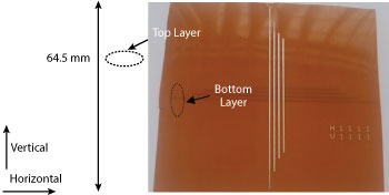
Figure 1 Photograph of the printed chipless RFID tag.
To date, the only commercially available and successful TDR chipless RFID system is surface acoustic wave (SAW) based (developed by RF SAW®).3 Although operational, SAW tags are not fully printable and planar due to their piezoelectric nature and hence cannot be applied to banknotes, postage stamps or other paper or plastic items. Printable TDR based chipless tags have data capacity and size limitations due to the long delay lines required for data encoding.4
Printable spectral signature (frequency encoding) tags have been published in significantly higher numbers by researchers due to their compact size, multi-bit capacity and reading range compared to TDR based tags. The earliest version of a multi-bit 35-bit chipless tag was presented by Preradovic et al.,5 using a basic presence or absence of resonance for representing logic 0 and 1, respectively. A further increase in data capacity was introduced by Vena et al.,6 with a reduced size and a novel encoding technique based on resonance shifts within a certain frequency band representing different binary codes. Islam et al.,7 further increased data encoding by using orthogonal polarizations (polarization diversity). Polarization diversity can only apply to applications where the tag’s orientation and placement is constant and/or known at all times. If the code is repeated in both polarizations, the tag is orientation insensitive; however, the data capacity is reduced by half.8 Chipless tags insensitive to polarization presented by Shen and Law9 use circularly polarized scatterers that do not have orientation restrictions.

Figure 2 Photograph of screen printed ink at 10 µm and 0.8 µm on a 50 µm polyimide film.
All of these works describe tags that contain copper. The purpose of chipless RFID is to reduce the cost of the tag to a fraction of a cent. This makes copper unacceptable in a final solution. Conductive inks and pastes offer cheaper and easier ways to print tags, but performance is compromised due to their comparatively lower conductivities. So far, three types of printing techniques have been used: ink-jet, screen printing and flexography. Work on ink-jet printed chipless tags with three scatterers and a total of 6 bit encoding capacity is presented by Vena et al.10 Work on screen printed chipless tags with 3-bit data capacity using the presence and absence of resonances is presented by Nair et al.11 Tags printed using flexography on paper with five resonators for encoding have been reported by Vena et al.12
This article describes a novel chipless tag that has overlapping dipole resonators printed in multiple layers, with orthogonal polarizations, on a low cost substrate. The tag enables the use of 3D resonator placement for efficient use of space and enhances the tag’s application as a security feature. The resonators are printed using screen printing. We investigate the effect of different conductive ink thicknesses on the performance of the tag, tag orientation and the isolation between overlapping orthogonally polarized resonators. This is developed mainly for security and anti-counterfeiting applications, where its multilayer aspect does not automatically identify the true nature of the layout and therefore creates ambiguity for counterfeiters. It has been patented.
Operating Principle
Figure 1 is a photograph of the chipless RFID tag. This prototype operates between 1.8 and 3 GHz; if required, it can be designed to operate higher in frequency by reducing its dimensions. It contains linearly polarized, shorted dipoles printed in orthogonally polarized orientations separated by a dielectric layer. The tag has two layers but one can easily add more, depending on the application. It employs dual polarization to either encode more data or enable the tag to be orientation insensitive.
To enhance data capacity, orthogonal polarization is achieved by printing a set of dipoles with vertical polarization and a set of dipoles with horizontal polarization. In order to interrogate the tag, the RFID reader sends a signal in both polarizations when polarization diversity is employed for encoding or in a single polarization when it is not. Since isolation between orthogonally polarized signals is very high, signals with orthogonal polarizations can be transmitted at the same time to reduce reading time. Each shorted dipole has a resonance which acts as a stopband filter when the tag is placed between two reader antennas. The number of bits depends on the encoding technique. A simple presence or absence of resonance gives a maximum capacity of 8 bits with each resonator encoding 1 bit. With the encoding technique presented by Vena et al.,6 it can be increased depending upon the reader’s frequency resolution and tag resonator separation.
Design
Tag Substrate and Printing
The tag is printed on a low cost polyimide thin film (εr = 4.8, h = 50 μm, tan δ= 0.04). Using screen printing, conductive paste is deposited in various thicknesses. Figure 2 shows measured thicknesses of 10 and 0.8 µm using a microscope. Figure 2 indicates that the thickness of the ink can vary 15 percent from the desired thickness so it is important to measure more tags and average the results.
Tag Resonators
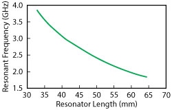
Figure 3 Simulated dipole resonant frequency vs. resonator length.
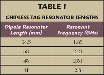
The tag resonators are used to encode data by resonating at different frequencies. Table 1 shows the relationships between the lengths of the resonators used in the tag from Figure 1 and their resonant frequencies. A parametric study of physical parameters using Ansys HFSS is used to optimize their resonant frequencies (see Figure 3). The resonators are evenly spaced at ~300 MHz.
A figure of merit for another parametric study is the attenuation created by each resonator. Better performing resonators attenuate stronger at their resonant frequencies. The tag is placed between two reader antennas at a distance of 5 cm from each antenna. The reader antennas are ultra-wideband, low gain disc monopoles. The near far field region for the monopole antennas is calculated to be at ~2 cm.
After setting the length of the resonators, we investigate the effect of printed conductive ink thickness. We calculate that the conductivity of the ink is approximately 3 × 10⁶ S/m. The resonator is set to a length of 64.5 mm resonating at 1.85 GHz. Figure 4 shows the variation of resonator attenuation with ink thickness. As expected, the thicker the deposition of the conductive ink, the greater the attenuation. Below 4 µm the attenuation of the resonator drops below 10 dB. Below 1.5 μm the attenuation starts dropping faster due to the skin effect. The recommended ink thickness is above 6 μm based on the results shown in Figure 4.

Figure 4 Measured resonator attenuation vs. ink thickness.
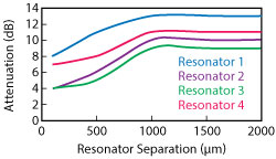
Figure 5 Measured resonator attenuation vs. resonator separation.
The relationship between dipole resonator separation and width is presented in Figures 5 and 6. We set the printed conductive ink thickness to 10 μm. Placing the resonators next to each other causes them to couple. It is first required to understand the minimum separation between resonators before coupling starts affecting performance. Figure 5 shows that the minimum required separation is 1000 μm. Figure 6 shows the response of the resonators for different widths. With the width of the resonator varied from 100 to 500 μm, a linear relationship between attenuation and width is observed.
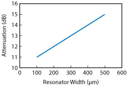
Figure 6 Measured resonator attenuation vs. resonator width.
MEASUREMENT
Setup
The experimental setup block diagram and photograph are shown in Figures 7 and 8, respectively. The reader antennas are linearly polarized Vivaldis. Vivaldi antennas exhibit wide bandwidths, directional radiation patterns and high gain. The tag is placed 10 cm away from each reader antenna. An Anritsu vector network analyzer, transmitting -10 dBm power, is the reading instrument. S21 is measured with and without the tag placed between the reader antennas. The value of S21 when the tag is not present is used to calibrate and normalize the tag received signal.
Cross-Polarization Encoding
In this mode, the chipless RFID tag uses polarization encoding to enhance the number of resonances used to encode data and therefore enhance its data capacity. The application of the tag in this case is orientation sensitive and must be known to align reader antenna polarization.
Figure 9 shows the tag’s normalized received signal. It encodes the data using three resonances in the vertical polarization and one resonance in the horizontal. Resonances are removed simply by not printing the dipole resonator. As shown in Figure 9, resonators with orthogonal polarizations do not appear in the response. We can conclude that polarization isolation is high and that it is possible to have good isolation with the resonators overlapping and separated by a thin 50 μm dielectric.
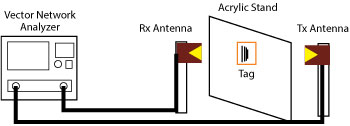
Figure 7 Chipless RFID tag measurement setup.
Orientation Insensitive Encoding
If the application requires an unknown tag orientation, or one that is not fixed, then the dual polarization behavior can be made polarization insensitive by encoding the same code in both polarization planes. Figure 10 shows the response of the tag at angles of 0, 45 and 90 degrees, respectively. In all three orientations the tag response remains reasonably constant and uniform.
Distance
Figure 11 shows the chipless RFID tag response at different distances from the reader antennas. A chipless tag with four printed resonators is used. A comprehensive study has been reported by Nair et al.,11 on conductive ink printed tags for reading ranges up to 100 cm. In this work, we go out to 20 cm, which should be acceptable for anti-counterfeiting applications such as banknote authentication. From Figure 11, it is apparent that no resonant frequency shifts occur with the change of distance; as expected all that changes are the amplitudes.
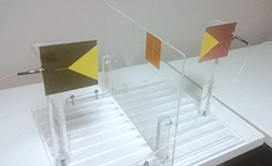
Figure 8 Photograph of chipless RFID tag measurement setup.

Figure 9 Measured received signal from tag 10110100 at 10 cm.
Conclusion
A novel chipless RFID tag with 3D stacked dipole resonators printed on a thin 50 µm polyimide film is the first tag with overlapping multilayer resonators to be successfully developed and tested. A parametric study of the tag’s performance with varying resonator length, width, conductive ink thickness, orientation changes, polarization and reading range is presented. The tag operates between 1.8 and 3 GHz and can produce four or eight resonances for data encoding depending upon the application. For higher data capacity and orientation sensitivity the tag uses polarization diversity to encode the data. For orientation insensitive applications the tag encodes the same data in both orthogonal polarizations in order to be readable in any orientation. The tag is printed using a low cost screen printing technique, on low cost polyimide film with a lossy conductive ink with 3 × 10⁶ S/m conductivity, almost 20 times lower than copper. We have demonstrated that the tag is fully operational and has the potential to enhance anti-counterfeiting of banknotes and other paper/plastic items.
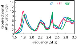
Figure 10 Tag 1111 measured code at 10 cm for different rotations.
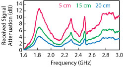
Figure 11 Tag 1111 measured code at various distances from reader antennas.
References
- S. Preradovic, N. Karmakar and I. Balbin, “RFID Transponders,” IEEE Microwave Magazine, Vol. 9, No. 5, October 2008, pp. 902103.
- S. Preradovic and N.C. Karmakar, “Chipless RFID: Bar Code of the Future,” IEEE Microwave Magazine, Vol. 11, No. 7, December 2010, pp. 87297.
- C.S. Hartmann, “A Global SAW ID Tag With Large Data Capacity,” IEEE Ultrasonics Symposium Proceedings, Vol. 1, October 2002, pp. 65269.
- S. Shrestha, M. Balachandran, M. Agarwal, V.V. Phoha and K. Varahramyan, “A Chipless RFID Sensor System for Cyber Centric Monitoring Applications,” IEEE Transactions on Microwave Theory and Techniques, Vol. 57, No. 5, May 2009, pp. 130321309.
- S. Preradovic, I. Balbin, N.C. Karmakar and G.F. Swiegers, “Multiresonator-Based Chipless RFID System for Low-Cost Item Tracking,” IEEE Transactions on Microwave Theory and Techniques, Vol. 57, No. 5, May 2009, pp. 141121419.
- A. Vena, E. Perret and S. Tedjini, “Design of Compact and Auto-Compensated Single-Layer Chipless RFID Tag,” IEEE Transactions on Microwave Theory and Techniques, Vol. 60, No. 9, September 2012, pp. 291322924.
- M.A. Islam and N.C. Karmakar, “A Novel Compact Printable Dual-Polarized Chipless RFID System,” IEEE Transactions on Microwave Theory and Techniques, Vol. 60, No. 7, July 2012, pp. 214222151.
- A. Vena, E. Perret and S. Tedjini, “A Depolarizing Chipless RFID Tag for Robust Detection and its FCC Compliant UWB Reading System,” IEEE Transactions on Microwave Theory and Techniques, Vol. 61, No. 8, August 2013, pp. 298222994.
- Y. Shen and C. L. Law, “A Low-Cost UWB-RFID System Utilizing Compact Circularly Polarized Chipless Tags,” IEEE Antennas and Wireless Propagation Letters, Vol. 11, October 2012, pp. 138221385.
- A. Vena, A. A. Babar, L. Sydanheimo, M. M. Tentzeris and L. Ukkonen, “A Novel Near-Transparent ASK-Reconfigurable Inkjet-Printed Chipless RFID Tag,” IEEE Antennas and Wireless Propagation Letters, Vol. 12, June 2013, pp. 7532756.
- R. Nair, M. Barahona, D. Betancourt, G. Schmidt, M. Bellmann, D. Hoft, D. Plettemeier, A. Hubler and F. Ellinger, “A Fully Printed Passive Chipless RFID Tag for Low-Cost Mass Production,” 8th European Conference on Antennas and Propagation, April 2014, pp. 295022954.
- A. Vena, E. Perret, S. Tedjini, G. Tourtollet, A. Dellatre, F. Garet and Y. Boutant, “Design of Chipless RFID Tag Printed on Paper by Flexography,” IEEE Transactions on Antennas and Propagation, Vol. 61, No. 12, December 2013, pp. 586825877.