
Selecting a common mode choke usually comes with more issues than might be expected. The selection process involves evaluating a range of different filter characteristics and aligning them with the desired system specifications. The aim of this application note is to help the design engineer to choose the right filter for the application and explain some concepts that are important when choosing a suitable filter for the requirements of a given system. These include matching impedances as well as considering the adequate cutoff frequency, and differential and common mode attenuation.
A number of ‘eye diagrams’ are referred to, which are composed of an overlay of several data frames to give an indication of how a component or transmission line changes the waveform of a transmitted signal. Statistical data frame overlays are used, which reveal reflections on the line, phase shifting as well as added signal noise.
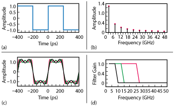
Figure 1 Effect of different filters on a digital signal under idealized conditions.
Most digital signal standards such as USB or HDMI define a mask to fit into the free area of the eye diagram, thereby establishing limits for the minimal eye opening or signal shape. This translates into both the minimal voltage level needed to avoid signal decoding errors and the minimum signal width or time period for the digital symbol to be maintained to avoid signal decoding errors. Both parameters are important indicators for the integrity of a given signal. The eye diagrams shown were measured on a network analyzer with Time Domain Reflectometry (TDR).
Cutoff Frequency
A low pass filter’s cutoff frequency (fc) is defined as the frequency at which the filter attenuates the amplitude of the signal by 3 dB. A 3 dB attenuation reduces the power of the input signal to half of its original value. This frequency is also known as f3dB. Figure 1 demonstrates the effect of a series of low pass filters with different cutoff frequencies under ideal conditions. Figure 1a shows the input signal and Figure 1b the signal’s harmonics. Figure 1c shows the signal’s output shape after the filters — the color of each of the lines corresponds to the filter — the frequency response of which can be seen in Figure 1d. This graph also reveals which of the input signal’s harmonics are being filtered by the individual filters. Their f3dB values are 9, 14 and 26 GHz, respectively.

Figure 2 Trace configuration.
In order to retain the integrity of a signal, it is recommended not to filter its first four harmonics. In keeping with this, the cutoff frequency should be greater than the fourth harmonic frequency of the signal. For a square wave, this is four times its base frequency.
Transmission parameters
The next step would be to put all this together and look into a typical product catalogue to identify a filter that is the best fit for the application. However, this might not be quite as easy as expected: Some parameters — notably the cutoff frequency — do not appear in many of these compilations. Instead of the attenuation in differential and common mode, impedance values in both modes are given, so finding the right common mode choke might be a bit of a challenge. However, the specifications do include graphs and these will help find the right filter if used in the right way.
The graphs included in such a catalogue tend to be closely related, meaning that when the attenuation of a component increases the impedance will also increase. However, a closer look into the specification details can reveal other ways to retrieve the desired attenuation values.
The main way to derive a filter’s attenuation is by means of its scattering parameters, which provide transmitted and reflected signal ratios. There are two ways of representing these parameters; as scattering parameters or as mixed mode scattering parameters.
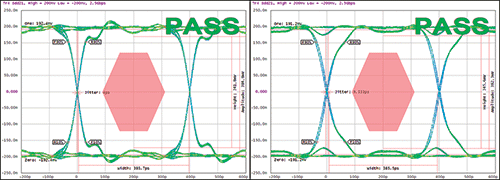
Figure 3 Reflection effect of common mode chokes in differential mode visualized with eye diagrams.
The single ended scattering parameters represent the relationship between input and output levels using different test configurations for the common and differential modes. These test configurations or test fixtures deliver good approximations of the attenuation of a filter up to a few gigahertz but for frequencies beyond 3 GHz these approximations may not be valid.
Mixed mode S-parameters are four wire type measurements. With reliable measurement in the high frequency components, there is no need for extra approximation to be done. It is possible to send a differential signal through the coaxial cables and see the effect of the circuit on this signal. Furthermore, it is possible to measure the attenuation of a common mode signal or the conversion between common and differential modes. This measurement method yields the mixed mode scattering parameters, SDD for the differential mode and SCC for the common mode, while the general S-parameters do not differentiate between differential or common mode unless certain other SMD test fixtures or approximations are used.

Figure 4 Filter setup.
Transmission line impedances
When considering the requirements for a differential data line there are certain terms used such as characteristic impedance, differential mode impedance, or common mode impedance. The characteristic impedance of a line is the relationship between the amplitudes of oscillating voltages and currents travelling through the line. This value is calculated in a line without reflections, so the length of the line has no influence on it.
The common mode and the differential mode impedances depend on the characteristic impedance (Zo) and the coupling factor between traces (k). To clarify the meaning of these two impedance values, this note will explain the meaning of the terms odd mode impedance (Zodd) and the even mode impedance (Zeven).
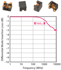
Figure 5 First Filter: WE-CNSW HF 0504 (7442335900) characterized by the mixed scattering parameters.
Figure 2 shows a trace configuration in a differential transmission line. From this configuration, the applied voltage in each trace can be calculated as:
V1 = Z1i1 + Z1ki2
V2 = Z2i2 + Z2ki1
If the transmission is balanced and the traces are designed carefully
i1 = -i2 and Z1 = Z2 = Z0
Under these assumptions, the first two equations can then be rewritten as:
V1 = Z0i1 – Z0ki1= i1(1 – k)Z0
V2 = Z0i2 - Z0ki2 = i2(1 - k)Z0
Rewriting the equation to show Zodd results in:
Zodd = (1 - k)Z0
In unbalanced transmission mode the following applies:
i1 = i2
Z1 = Z2 = Z0
So the applied voltages in the traces can be rewritten as:
V1 = Z0i1 + Z0ki1 = i1(1 + k)Z0
V2 = Z0i2 + Z0ki2 = i2(1 + k)Z0
This results in Zeven as:
Zeven = (1 + k)Z0
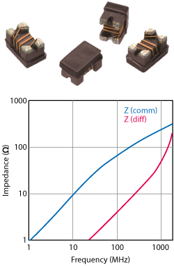
Figure 6 Second Filter: WE-CNSW 0805 with impedance curve of 744231091.
Once Zeven and Zodd have been calculated it is easier to define the differential and common mode impedances. It is assumed that both lines are connected to ground at the end. In differential mode, the fact that i1 = - i2 is made use of, which means there is no current flowing to ground. This leaves the impedance between the two lines equal to the Zodd values of each trace connected in serial:
Zdiff = 2Zodd = 2 (1 - k)Z0
This explains why the impedance in differential mode can be much higher than the characteristic impedance.
Now, making the same assumption for the common mode and taking into account that i1 = i2, meaning that all current will flow through ground, establishes the common mode impedance as equal to the Zeven values of each line connected in parallel:
Z comm= 2 Zeven = (1+k)Z0/2
Impedance Matching
In order to reach the maximum power transfer the impedances involved should be considered. When designing a circuit the aim should be to match the source impedance with the load impedance as a necessary condition to avoid reflections that might disturb the signal.
However, when a new component is added the impedance of the system will change and there may be undesirable reflections. The best filter to insert into the system would be one with no differential mode impedance at the operating frequency but this is impossible in practice. Because of this, a filter is required with as low a differential mode impedance in the desired frequency range as possible.
The target for the common mode choke is to balance the differential signal, which means that the signal power levels in both lines should be the same but with opposite signs. To reach this goal the common mode interference portion must be removed without affecting the integrity of the differential signal. This is why it is essential to look for a common mode choke that offers higher common mode impedance and lower differential mode impedance in the desired frequency range.
Figure 3 illustrates the effect of a common mode choke on a digital signal at 5 Gbps with Non Return Zero (NRZ) modulation. Some reflections still appear when the filter is inserted because of a small impedance mismatch on the transmission line. However, this mismatch does not dramatically affect the shape of the signal, allowing the eye diagram to pass a suitability test with a mask as required. It is important, however, to keep in mind that the negative effect will increase with frequency and component impedance.
The higher the operating frequency and the impedance of the filter, the greater the effect on the signal eventually resulting in total information loss due to reflections and attenuations occurring in the line due to an unsuitable filter. Common and differential mode impedances are related to each other and are governed by the component’s physical properties and geometry. For any one choke series with a specific core size, higher common mode attenuation will come with higher differential mode attenuation.
The following key principle applies: The lower a choke’s differential mode impedance, the smaller the effect on the signal but it will never disappear completely. There are no perfect or ideal filters but a good component selection will help avoid surprises.
Figure 7 Third Filter: WE-CBF HF with impedance curve of the 74286314.
Filter analysis
To see how the differential mode attenuation affects the signal shape consider three filters, each using a different type of component. The filters are inserted into a differential line with 50 Ω characteristic impedance and 90 Ω differential impedance. The architecture setup is shown in Figure 4. The components used to build the filters and the characterizations of graphics are shown in Figures 5, 6 and 7.
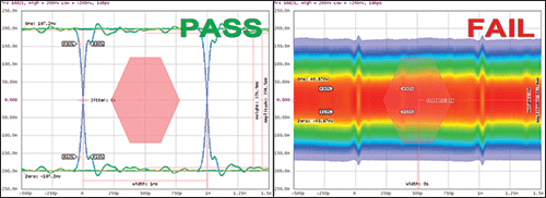
Figure 8 Comparison between the line without filter (left) and the line with WE-CBF HF filter (right).
Eye diagrams obtained for different data rates are compared in figures 8 to 11. The signals are NRZ coded and the data rates are 1, 2.5, 5 and 7 Gbps. Figure 8 shows the effect obtained with a filter using ferrite beads as shown in Figure 7. Such a filter will deform the signal dramatically. The ‘eye’ is completely closed and the test fails. The ferrite beads do not distinguish between the differential and the common mode signals so the carrier signal disappears along with the noise. These ferrite beads have a really good performance when used for a lower data rate as a differential mode filter, but if they are not designed for this function they will not give as good a performance as a common mode choke.
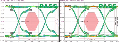
Figure 9 Eye diagram with the standard filter (left) and the high frequency filter (right) at 5 Gbps.
Focusing the attention on the comparison between the WE CNSW (standard type), and the WE CNSW HF (high frequency type) it is easy to see how the cutoff frequency affects the signal with the effects on the standard type (left side) and the high frequency type (right side) shown. Both components have almost the same impedance in common mode. The main difference is in the differential mode impedance. Comparing the effect at 5 Gbps in Figure 9, it is possible to see that the standard type has a lower cutoff frequency than the high frequency type.
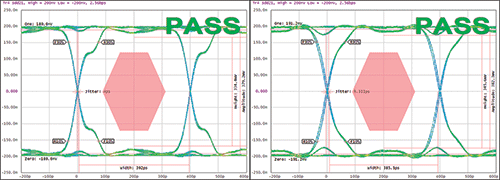
Figure 10 Eye diagram with the standard type choke (left) and the high frequency type choke (right) at 2.5 Gbps.
At 2.5 Gbps the difference is smaller as can be seen in Figure 10. The signal’s critical harmonics are filtered by neither the high frequency component nor the standard component. In both cases the signal is not strongly affected by the component because both filters are designed to have low differential impedance. But increasing the data rate of the signal will also increase the harmonics and the number that are being filtered. The cutoff frequency of the standard type is about 2 GHz, whereas with the high frequency type the cutoff frequency is at least doubled, conserving the impedance value in common mode.
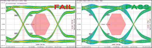
Figure 11 Eye diagram with the standard type choke (left) and the high frequency type choke (right) at 7 Gbps.
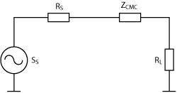
Figure 12 The circuit used to show the relationship between the choke’s impedance and the resulting attenuation.
In Figure 11 the different eye diagrams at 7 Gbps for both filters are shown. In case of the standard type the base frequency of the signal is also affected and attenuated. However, with the high frequency type, only the high frequency harmonics are attenuated, resulting in good results for the eye diagram test.
There are several important factors to take into account when building a filter. However, not all of them can be derived from the impedance curve alone. Depending on the underlying measurement method, data sheets will show the impedance curve, the attenuation curve, or the scattering parameters curve. There is, however, always the possibility to extract the information needed to choose the right common mode choke for the desired filter application, even if this information is not shown explicitly in the datasheet.
Figure 12 shows the equivalent circuit of the system in differential mode. The source (RS), the load (RL) and the choke (ZCMC) impedances are present in the equivalent circuit. For a perfect match the load impedance should be the conjugate of the source impedance (same real part, opposite imaginary part) and the choke impedance should be zero. This last requirement is not possible with real components. Keeping the source and load impedances constant it is possible to calculate the attenuation added by the component:
Zcomm=2Zeven=(1+k)Z0/2
To simplify the calculation and proceed directly to the important point the choke impedance is considered to be imaginary. This approximation will give the ratio in the worst case. Figure 13 shows the effect of the relationship between the choke’s and the load’s impedance on the attenuation.
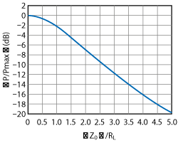
Figure 13 Effect of the choke impedance on the attenuation.
By designing circuit with a common mode choke in mind it is possible to adapt the impedances to reduce the attenuation of the filter. The complexity of the matching circuit will increase, but the effect of the filter on the differential signal will be reduced.
Conclusion
This note affirms that a high frequency choke will be always more appropriated for high frequency applications and it should be used for circuits with a differential mode line with a high speed data rate. The size, attenuation or impedance depend on the application. And once the relationship between the different parameters is known, it should be possible to estimate the effect of the choke on the differential data line, irrespective of the way this information is shown.
In a first approximation to choose the appropriate choke, the application must be located in a frequency range. Once the cutoff frequency is decided, the choke family that will be chosen depends on the important parameters for the design. For example, if the application has a signal with harmonics in frequencies higher than 1 GHz a high frequency choke should be used, offering good attenuation at the high frequencies, with a broad transmission bandwidth, which means, the impedance in differential mode is negligible up to 8 to 10 GHz. Once the match code has been decided, the next step is to decide on the size, which depends on the rated current, DC and AC impedance, etc.