
While it is widely held that S-parameters alone combined with harmonic balance (HB) cannot simulate the power performance of transistors, this article describes a method for designing and simulating amplifiers for maximum power using HB simulation, when the only available data is transistor S-parameters. The method is widely applicable when nonlinear transistor models are not available. It can also be very helpful even when the nonlinear models are available.
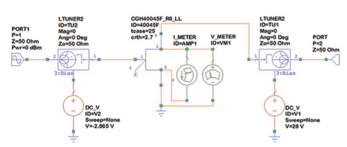
Figure 1 Output stage in Microwave Office.
The amplifier design methodology described here is an extension of Steve Cripps’ load line approach,1-3 which was extended with the power parameters introduced by Pieter Abrie.4 These techniques may be used to create useful approximations that allow HB simulation with transistors that do not have nonlinear models. This paper is a sequel to an earlier paper presented in April 2013 at ARMMS.5
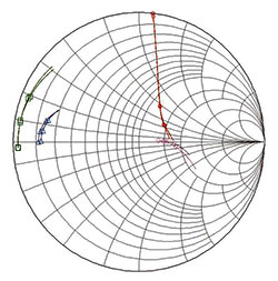
Figure 2 Fitting a linear model to the S-parameters in MultiMatch.
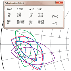
Figure 3 Load-pull contours extracted in MultiMatch.
Cripps’ original paper was published in 1983 when HB simulation was not yet in use and load-pull measurements were the only option available for device characterization. When Cripps’ technical note was published, HB simulation was available but, among other problems, was very slow. The Cripps approach offered a much simpler way to design for high power. Cripps expressed a hope that the simple math of his approach should be incorporated in the general linear simulators “in much the same way that most of the currently available packages compute noise figure.”2 He also stated that with “some slightly innovative use” the approach could be applied when there is feedback, for multi-stage design and, potentially, for other amplifier configurations. Unfortunately, his approach was never implemented in any of the general simulators. It was, however, implemented in a more advanced form in the specialized MultiMatch Amplifier Design Wizard6 developed by Pieter Abrie. Abrie presented the power parameters in his book4 and implemented them in MultiMatch for the design of Class A and Class AB amplifiers.
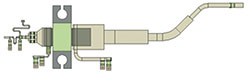
Figure 4 Output stage layout in Microwave Office.
The mapping functions of the power parameters lifted any restrictions associated with the transistor’s configuration, including feedback, resistive loading, grounding node position, parallel cells or chips, reference plane issues and multiple stages. There are interesting similarities with the noise parameters, such as series feedback allowing easier matching for maximum power.
Today, the HB simulations are as fast as the linear simulations were 20 years ago. While accurate nonlinear transistor models have been developed, they are still not provided for many useful transistors. Abrie’s power parameters approach is a fully developed method which can easily be incorporated in any of the general simulators to speed up and enhance the design process for P1dB and Psat, especially when nonlinear models are not available.
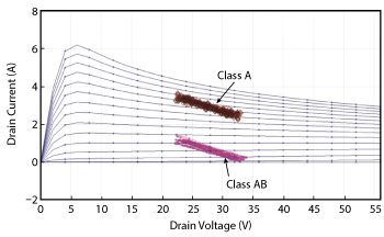
Figure 5 I-V curves and Class A and AB DLLs at low output power.
0.5 to 2.5 GHz GaN PA DESIGN
The streamlined HB process6 was used to design a three stage power amplifier covering 0.5 to 2.5 GHz, using a 45 W GaN HEMT. In addition to the design process, the results of the HB simulations of the dynamic load lines for each stage will be shown. This will enhance the understanding of the design process and explain how to extract the desired power from a transistor stage when a nonlinear model is not available.
Figure 1 shows the start of the design output stage design in the NI AWR Microwave Office® simulator. The nonlinear model of the transistor and the tuners could be used to extract the impedances for maximum power and gain over the frequency band. Instead, only the S-parameters at the transistor’s Imax/2 are extracted. The S-parameters are then imported into MultiMatch to fit a linear model (see Figure 2). After defining the maximum current and voltage areas on the I-V curves (the clipping boundaries), the power parameters are used to extract the load-pull data (see Figure 3). Then the output network is synthesized to provide the load impedance associated with the maximum pre-clipped power, followed by the input matching networks to provide maximum flat gain and stability. The MultiMatch layout is easily manipulated to the desired form, and the schematic and the layout are exported to Microwave Office (see Figure 4). With Microwave Office, the microstrip discontinuities are fully simulated, using either electromagnetic models or full electromagnetic simulation of parts of the layout. The nonlinear model and HB are used to simulate the powers of the fundamental and harmonic signals, the associated gain and gain compression, currents, voltages and efficiency. Using these simulations, small adjustments are made to achieve the best performance. After the output stage design is finalized, two are combined with hybrid couplers to form a balanced output.
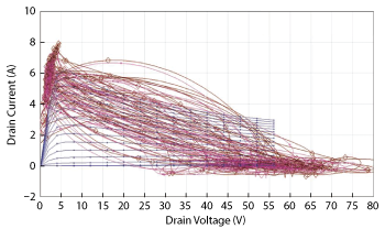
Figure 6 I-V curves and Class A and AB DLLs at Psat.
Cree supplied nonlinear models for the GaN HEMT used in the design, with access to the voltage and current across the intrinsic generator, as shown in Figure 1. The simulation of the voltage and current – the dynamic load line (DLL) – across the intrinsic generator provides better visualization, understanding and design capability. The simulated DLLs across the band for Class A and Class AB biasing at low power levels are plotted in Figure 5, showing that Class A biasing provides the maximum voltage and current swing, hence maximum Psat. Compare these DLLs with the Class A and Class AB DLLs at Psat (see Figure 6). Figure 7 shows the Class A and Class AB Psat and power-added efficiency (PAE) simulations across frequency, with about the same results for the two bias conditions. This illustrates the validity of the design method.
The two-stage driver design uses a Cree GaN HEMT at the output, for which a nonlinear model is available, driven by a GaAs HFET, with only S-parameters at a Class A bias point. The S-parameters of the GaN transistor were extracted in Microwave Office, and the S-parameters of the GaAs transistor were used in MultiMatch to create linear models for these transistors. With the voltage and current boundaries defined, the power parameters and synthesis were used to design the two driver stages to provide maximum power and flat gain across the band.
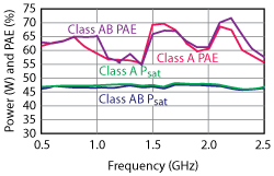
Figure 7 Class A and Class AB Psat and PAE simulations.
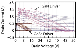
Figure 8 I-V curves and the DLLs of the GaN and GaAs driver stages.
The driver schematic was imported into Microwave Office, and the S-parameters of the two transistors were replaced with the nonlinear model for the Cree GaN transistor and the linear model for the GaAs HFET. Voltage and current meters were placed across the intrinsic generators, with an M-probe at the output of the GaAs transistor. The nonlinear model was used to simulate the I-V curves and the DLLs of the GaN transistor stage (see Figure 8). Superimposed in the lower left corner of the plot are the boundaries that define the pre-clipped maximum voltage and current swings of the GaAs transistor. The DLLs are shown inside these boundaries.
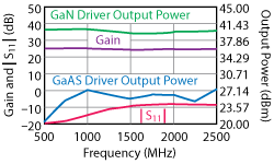
Figure 9 Simulated output power, power gain and input return loss of the driver as well as the output power of the GaAs transistor.
These load lines were simulated using the HB simulator and the linear model of the transistor. The input power levels were selected and tuned so that the DLLs of the GaAs transistor stage just reach hard clipping. Figure 8 shows that the GaAs transistor is starting to compress after the GaN transistor is already in deep compression. The pre-clipped output power is typically 0.5 to 1 dB below P1dB. This confirms that the GaAs stage has sufficient power to drive the GaN stage. The linear model of the GaAs transistor was extracted from the S-parameters in a special facility in MultiMatch. It is also possible to do this in Microwave Office. For the GaAs transistor, only the S-parameters were available; after using them to extract a linear model, the HB simulation was used to simulate and predict the pre-clipped maximum Class A output power. Figure 9 shows the simulated driver output power, power gain and input return loss as well as the output power of the GaAs transistor, measured by the M-probe.
This method of simulating the DLL and the pre-clipped output power is also very useful when it is important to provide proper loading to each cell of a multi-cell transistor or when multiple transistors are connected in parallel, as is typical in MMIC power amplifiers. Optimization for the correct DLL is much faster when linear models are used. This is important because the networks are typically very complex, and the input networks also need to be optimized to provide equal drive. Typically, MMIC design kits provide linear and nonlinear models. Optimizing the initial circuit by using the linear models and checking the results using the nonlinear models provide for a better, faster and, arguably, more accurate design approach. The optimum load line for maximum output power can also be optimized relatively quickly using the nonlinear model of the transistor, if the input power for the simulation is low.

Figure 10 50 W, 0.5 to 2.5 GHz power amplifier.
The method of HB simulation of the DLL using the linear model can extract the optimum load impedance for maximum output power of Class A amplifiers and, arguably, Class AB amplifiers. The approach uses a linear transistor model driven by a tunable power source, an impedance tuner at the output and a gamma probe to place the impedance of the tuner on the Smith chart.
This power amplifier design was built (see Figure 10) and tested. The measured and simulated saturated output power are shown in Figure 11; in both cases, the output is approximately 48.5 dBm average. The measured and simulated large-signal gain are also similar, generally between 52 and 54 dB from 500 MHz to 2.5 GHz.
CONCLUSION
This article described a method for designing and simulating amplifiers for maximum power using HB simulation, when the only available data are the S-parameters of the transistors. The method is widely applicable, from low noise to high power amplifiers, narrowband to multi-octave. It can be used any time nonlinear transistor models are not available and the designer must know and design for the power deliverable by an amplifier stage. It is also useful when nonlinear models are available.
Pieter Abrie’s power parameters approach is fast and versatile, but it exists only in MultiMatch Amplifier Design Wizard. If the power parameters method is incorporated in the general-purpose simulators, it will complement this methodology and, in general, dramatically enhance RF/microwave amplifier design. For example, extracting full load-pull data and contours would be near-instantaneous in many cases. While it is desirable to incorporate the power parameters in the general-purpose simulators, the MultiMatch synthesis techniques and procedures are also required. These are the only real frequency and real world synthesis techniques available in a commercial software product. Incorporating them will provide unprecedented levels of productivity and creativity in the design of matching networks from inside the general-purpose simulators.
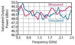
Figure 11 Measured vs. simulated saturated output power of the assembled amplifier.
The nonlinear models from Cree provide access to the voltage and current across the intrinsic generator, which gives deeper insight to these design methods and approaches and greater versatility using them. Qorvo GaN transistor nonlinear models developed by Modelithics also do so. Hopefully, this capability will be offered by other providers of linear and nonlinear models for RF/microwave transistors.
References
- S.C. Cripps, “A Theory for the Prediction of GaAs Load-Pull Power Contours,” IEEE-MTT-S International Microwave Symposium Digest, 1983, pp. 2212223.
- S.C. Cripps, “GaAs FET Power Amplifier Design,” Matcom Inc., Technical Note 3.2.
- S.C. Cripps, “RF Power Amplifies for Wireless Communications,” Artech House, 1999, ISBN 0-89006-989-I.
- Pieter L.D. Abrie, “Design of RF and Microwave Amplifiers and Oscillators,” Artech House, 2009, ISBN 978-1-59693-098-8.
- I. Boshnakov, A. Wood and S. Taylor, “RF & Microwave Solid State Power Amplifier Design is a Speciality,” ARMMS, April 2012.
- MultiMatch Amplifier Design Wizard, Pretoria: Ampsa (Pty) Ltd.; www.ampsa.com.