
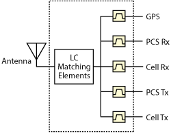
Figure 1 Quintuplexer comprising five filters with dissimilar passband frequencies.
In many parts of the world, smartphones have become an integral part of everyday life, and many users rely on their handsets as an easy way for going online. In the U.S., it is reported that in early 2011, one in three Americans owned a smartphone. As of 2015, that number has almost doubled.1 Projections indicate that in 2016 smartphone penetration will exceed 80 percent in the U.S.2 This continuous growth of smartphone popularity, and the expansion of its user base feeds the need for increased wireless data traffic, which has to be met with an increase in available bandwidth. The 3GPP standards body for mobile broadband specifies the spectrum of bands that can be used in wireless communications. Since the wireless spectrum is already crowded, and new chunks of wireless spectrum are hard to come by, 3GPP’s LTE-Advanced specifications identify carrier aggregation (CA) as one means to increase bandwidth over existing LTE frequency bands.3
With LTE, data traffic is aggregated in component carriers (CC) which are blocks of frequency spectrum 1.4, 5, 10 or 20 MHz wide. To increase the bit rate, CA means that up to five CCs can be aggregated, either within the same band or across different frequency bands. The number of downlink CCs must always equal or be greater than the number of uplink CCs. Since most of the wireless traffic demand is presently in the downlink (DL) direction, only one uplink (UL) CC is used, limiting carrier aggregation to the DL direction.
All smartphones on the market today already include the capability to transmit and receive on different frequency bands, for roaming purposes. However, enabling simultaneous operation of two separate LTE bands for CA puts additional constraints on the phone’s hardware components and data traffic management. In particular, inter-band CA with two frequency division duplex (FDD) LTE bands means that each transmit band now has two equally valid receive bands associated with it.
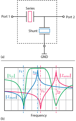
Figure 2 One stage half-ladder filter topology (a) with corresponding resonator impedances (Zseries, Zshunt) and filter response (b). Practical implementations of this basic filter topology use multiple stages.
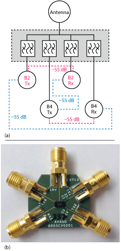
Figure 3 Band 2/4 quadplexer block diagram (a) and evaluation board (b). The dotted lines show high Tx/Rx isolation paths needed for carrier aggregation.
MULTIPLEXERS
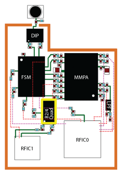
Figure 4 Band 2/4 quadplexer on the PCB of the RF front-end module.
Smartphones combine a lot of functionality into a relatively small package, and the size of any component inside the phone is limited. The RF front-end in a handset comprises all components between the antenna and the baseband/transceiver chips, such as frequency filtering devices, switches, power amplifiers, LNAs and a number of matching and routing elements. For any FDD band, a duplexer comprises two RF filters which ensure that the uplink transmit signal (Tx) does not interfere with the downlink reception (Rx). Integrating multiple non-overlapping filter bands into a single module (multiplexer) can reduce component count and the size of the phone’s RF front-end, as well as simplify and accelerate the integration into the phone. Introduced several years ago, multiplexers have become a standard way to optimize, miniaturize and simplify the filtering needs of multi-band phones, requiring only a single antenna to cover multiple bands without a switch between the antenna and the frequency filters.4 As an example, the functional block diagram of a quintuplexer is shown in Figure 1. Since CA requires different bands to be on at the same time (i.e., no switching between bands), a multiplexer is a convenient implementation to meet CA filtering needs.
Although common in earlier wireless generations, the RF front-end architecture of LTE phones no longer incorporates inter-stage filters between the transceiver and the PA in the transmit path. All FDD frequency filtering is now done by the duplexer or multiplexer, which puts stringent performance requirements on the filters. Any spurious signal from the PA toward the antenna needs to be rejected in the Rx path to not degrade phone sensitivity. This Tx/Rx isolation requirement in the duplexer specification is typically pegged at 55 dB minimum at the Tx and Rx frequencies. The filters inside the CA multiplexer must provide high Tx/Rx isolation, not only within a single FDD band but also across the different FDD LTE bands used in CA.
Driven by size and performance requirements, essentially all RF filtering devices in the handset incorporate surface acoustic wave (SAW) or bulk acoustic wave (BAW) resonator filter technologies. Both SAW and BAW technologies utilize piezoelectric resonators as the basic building block and are well established, mature technologies for RF filtering. For the filter designer, noteworthy SAW or BAW resonator properties are acoustic coupling (kt2) and Q-factor. Combining resonators to create a filter, Figure 2a illustrates a 1-stage half-ladder filter topology, a basic element for many filters. This configuration forms a passband when the series resonator has a higher resonance frequency than the shunt resonator (see Figure 2b). Based on this basic topology, any practical filter cascades multiple half-ladder stages to provide sufficient degrees of freedom to meet any realistic in-band and out-of-band filtering requirements. By doing so, the multi-stage filter arranges its poles within the passband, and the zeros outside its passband.
Combining two filters into a duplexer is the simplest form of a multiplexer. When combining RF filters into a CA-compatible multiplexer, there are two essential design constraints. First, all filters in the multiplexer must be matched at the common antenna node. For any of the passband frequencies, only the respective filter is terminated at the antenna port’s impedance Zant, to minimize RF reflections between the antenna and the multiplexer in the phone; all other filters must appear as open circuits, such that there is no signal leakage into any other filter path. Secondly, high Tx/Rx isolation, both in band and cross-band, is needed for CA use of the multiplexer. In the engineering of the multiplexer module, parasitic crosstalk or direct Tx/Rx signal leakage can degrade isolation and will need to be evaluated in the finished product. Both items need to be addressed in the CA-compliant multiplexer product design. Techniques to address these constraints are well understood.5,6 Finally, the filter designer uses circuit simulator software as well as 3D electromagnetic simulation to predict multiplexer performance.
BAND 2/4 QUADPLEXER
CA is being deployed in many locations around the globe and CA-capable multiplexers of corresponding LTE band combinations are emerging in the market. For the American wireless market, a recent implementation of a CA-compatible multiplexer is the Band 2 (1.9 GHz PCS) / Band 4 (1.7/2.1 GHz AWS) quadplexer (see Figure 3). Bands 2 and 4 are common North American FDD bands, and since carrier aggregation is already available in some locations,7 there is a tangible product need for such a quadplexer module. CA-compatibility underscores the value proposition of the Band 2/4 quadplexer module; however, the engineering is challenging for multiple reasons:
Band 2 Duplexer: The filter band gap (Tx/Rx) is relatively narrow, approximately 1 percent of the operating frequency between 1910 and 1930 MHz. Low insertion loss at both filter passband corners (Band 2 Tx high channel and Rx low channel) requires a sharp roll-off for both Tx and Rx filters. This is non-trivial, even without other filters multiplexed to the same antenna node.
Band 4 Duplexer: The filter passbands with low insertion loss are relatively easy to achieve, since the passband width is narrow and the Tx/Rx band gap is large. However, maintaining high Tx/Rx isolation over this large frequency gap can challenge manufacturing tolerances, since most of the signal suppression is purely electrical (L-C resonance, far from the acoustic zeros of the other filter).
CA-Compliance: High cross-band isolations are additional requirements on the filters (B4 Tx/B2 Rx, B2 Tx/B4 Rx, given the second multiplexer design constraint noted previously). Additional out-of-band attenuation requirements typically trade off against in-band performance (i.e., insertion loss) and need to be balanced carefully.
The passbands of the Band 2 and Band 4 filters are relatively close in frequency, with the Band 4 filter frequencies bracketing both Band 2 passbands. The antenna match cannot rely on a diplexer circuit to isolate filter bands; all filters in this quadplexer need be co-designed to optimize the antenna match and ensure high Tx/Rx isolation (all in-band and cross-band combinations).
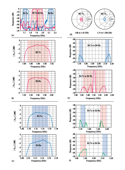
Figure 5 Measured performance of a Band 2/4 quadplexer showing the frequency coverage (a) Band 2 insertion loss (b) Band 4 insertion loss (c) Bands 2 and 4 Tx impedance match (d) in-band Tx/Rx isolation (e) and cross-band Tx/Rx isolation (f).
Increasing the number of filters connected to the same antenna node leads to increased insertion loss in each filter passband. This is unavoidable since the open circuit condition is never perfect or lossless (refer to the first multiplexer design constraint noted above). Elaborating on this point: to optimize multiplexer performance, it is not only helpful to reap low loss and high Q resonance performance of the resonator building blocks for good in-band filter performance, it is also helpful to garner low loss resonator performance at off-resonance frequencies. With low loss off-resonance performance, the open filter matching condition at the antenna port can be implemented with minimum parasitic loss and does not drain signal off the in-band performance of any passband. Using available SAW or BAW resonator filter technologies, part of the Band 2/4quadplexer optimization process is minimizing the losses of all four filters at all four passband frequencies.
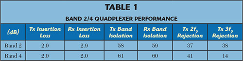
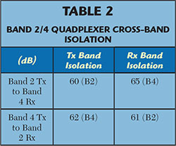
CA-compatible quadplexers for the Band 2/4 combination have been demonstrated by multiple suppliers, and some are available for sale. Figure 4 shows how the quadplexer would typically be integrated with the other RF components in the front-end of a smartphone. Measured performance of an Avago Band 2/4 quadplexer are shown in Figure 5 and the key performance parameters are summarized in Tables 1 and 2. The measured data reflects the recommended circuit matching elements.8
This quadplexer uses FBAR technology, a flavor of BAW resonator technology. FBAR is known for low loss resonators, both on and off resonance. Low loss fuels the performance of the quadplexer which, in turn, optimizes the phone’s performance and user experience: providing increased sensitivity and battery life, while benefitting from fast wireless data traffic using CA.
CONCLUSION
Smartphones continue to excel in popularity and market penetration, and their computing power and wireless connectivity are steadily improving. LTE-Advanced CA of different LTE bands is being rolled out to increase wireless data rates. As this deployment of band combinations continues across different geographies, corresponding CA multiplexers are emerging in the market. These components optimize RF performance, space and ease of integration for handset OEMs. Low loss filter technologies such as FBAR will continue to enable multiplexer performance. Higher levels of integration are feasible for future CA multiplexers, such as integrating three or more FDD bands. When designing such a multiplexer module, filter losses and antenna match need to be managed carefully to ensure an attractive product.
References
- A. Smith, “U.S. Smartphone Use in 2015,” Pew Research Center Internet & Tech, www.pewinternet.org/2015/04/01/us-smartphone-use-in-2015/, April 2015.
- H. Dediu, “Late Late Majority,” www.asymco.com/2014/07/08/late-late-majority/, July 2014.
- J. Wannstrom, “Carrier Aggregation explained,” www.3gpp.org/technologies/keywords-acronyms/101-carrier-aggregation-explained, June 2013.
- A. Chien, “Multiplexers for Multi-Band Wireless Handset Applications,” Microwave Journal, Vol. 50, www.microwavejournal.com/articles/print/5095-multiplexers-for-multi-band-wireless-handset-applications, July 2007.
- A. Link, “Innovative and Proven Approaches for Acoustic Filter, Duplexer and Multiplexer Design,” IEEE-IMS, WFF-3-362, Phoenix, Ariz., May 2015.
- T. Jamneala, P. Bradley, D. Feld, D. Clark and A. Chien, “A Generic Passive Matching Network for Multiplexers,” IEEE Transactions on Ultrasonics, Ferroelectrics and Frequency Control, June 2007.
- “LTE Carrier Aggregation Technology Development and Deployment Worldwide,” 4G Americas, www.4gamericas.org/files/8414/1471/2230/4G_Americas_Carrier_Aggregation_FINALv1_0_3.pdf, Oct. 2014.
- Avago B2–B4 quadplexer, ACFM-7024; www.avagotech.com/pages/en/rf_microwave/fbar_filters/multiplexers/acfm-7024/.