
A design methodology for a power amplifier (PA) with harmonic control is based on the simplified real frequency technique (SRFT). This is validated with a compact broadband power amplifier that has a maximum output power of 42.8 dBm and an efficiency of 55 to 70 percent in the 1.7 to 3 GHz band. With a 100 MHz LTE-A signal, linearization is accomplished using digital predistortion (DPD). With DPD linearization, -47.0/-48.5, -47.0/-47.7 and -47.6/-46.4 dBc ACLR are measured at 1.95, 2.15 and 2.55 GHz respectively at an average output power of 33 dBm.
Important components in communication systems, broadband power amplifiers must cover more and more frequency bands with low distortion to accommodate complex signal modulation. Common methods utilize Class J, continuous Class F and Class E operation,1-5 which include magnetic coupling networks, multistage ladder networks or the use of multiple transmission line sections (i.e., SRFT). Magnetic coupling and multistage ladder networks, however, employ a real-to-real resistance matching strategy that requires substantial tuning to match the PA’s complex output impedance. SRFT matching, on the other hand, uses a real to complex design methodology that provides a broadband matching structure without further tuning.

Figure 1 Output matching network simulation schematic.
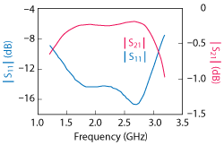
Figure 2 SRFT simulation results.
In a high efficiency/high power PA design, harmonic control is a critical factor. The original SRFT design process6-8 synthesizes a broadband transfer network in the fundamental region to meet the bandwidth requirement. This greatly simplifies the broadband PA design, but does not include harmonics.
This development combines the SRFT with harmonic control in matching a real 50 Ω load to the device’s complex output impedance. In this approach, the stopband frequency is swept and harmonic matching is carried out within the SRFT process. Matching network physical dimensions are obtained directly and employed without the need for optimization. For input matching, the device’s small resistive component and large reactive component make the Q too high to be matched over a broad band using common techniques; so, a resonator created with open and short circuited stubs is used to broaden the matching bandwidth.
A compact 50 × 60 mm broadband power amplifier in the 1.7 to 3 GHz band with a 10 W Cree CGH40010 GaN HEMT device is designed, built and tested. Experimental results show close agreement with simulation, while demonstrating the effectiveness of the design strategy.
Design and Implementation
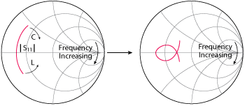
Figure 3 Short and open stub input matching.
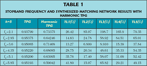
The load impedance is determined in ADS using the load-pull technique with CREE’s large signal model for the CGH40010 power HEMT over the fundamental band 1.7 to 3 GHz and the harmonic band 3.4 to 9 GHz. This is then used to define the transducer power gain (TPG) through the SRFT algorithm.6-8 The parameters of the SRFT program are set to provide a lowpass characteristic with five transmission line elements. The output topology is initialized and the objective TPG is set to 0.95. The frequency sweep across the stopband is run from 0.6 to 6.6 GHz and circuit parameters are optimized to obtain the best solution. In this sweep, the harmonic TPG (i.e., the TPG of the network by harmonic impedance) is calculated and averaged at all harmonic frequency points. This data is examined to ensure the matching network can support the required harmonic impedances. Finally, we choose fe =5.85 as the design parameter for the best harmonic control matching function.
The characteristic impedance of each transmission line element (see Table 1) is determined by normalization and Richard Extraction. For the selected PCB material (εr = 3.5), the physical length of every transmission line element is determined to be 6.85 mm by Equation 1.

where µ = µrµ0 and ε= εrε0 denote the permeability and permittivity of the substrate and τ denotes the actual delay of every transmission line element.
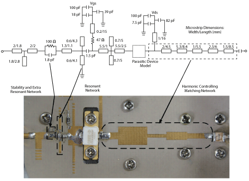
Figure 4 GaN PA schematic and implementation.
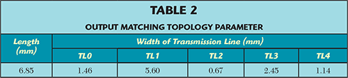
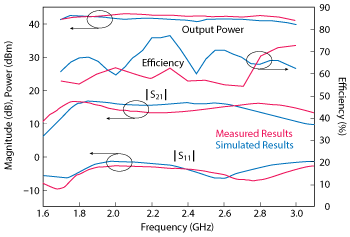
Figure 5 Measured vs. simulated performance.
For the stopband, a compact sized output matching network is realized. This network is tested with the complex fundamental impedance obtained through load-pull in ADS and its schematic is shown in Figure 1. From the simulation results (see Figure 2), the network exhibits a maximum of 0.4 dB loss over the 1.7 to 3 GHz frequency band.
For stability, an RC network is added to the input circuit, a 100 Ω resistance in parallel with a 1.8 pF capacitor. A very slim transmission line is employed for the internal connection as an inductive component to provide an additional RLC resonance. In addition, paralleled short and open stubs are used to broaden the bandwidth of the input match by twisting the input S11 curve on the Smith Chart around the center frequency. This is shown in Figure 3. Using the resonant network, the knotted curve can be easily matched to the 10 dB return loss circle on the Smith Chart.
Implementation and Measurement
The broadband compact GaN PA is shown in Figure 4. Its size is just 50 × 60 mm. The output matching structure, determined by the SRFT process, is shown in the Table 2. After adding the bias networks, further optimization of the output matching and input matching circuit is carried out. It is fabricated on a TACONIC RF-35 substrate with copper metallization. To reduce the transformation loss and provide a precise parasitic model for simulation, capacitors of ATC 100B series and 600S series are chosen. The circuit is characterized with both continuous wave (CW) and modulated signals to evaluate.
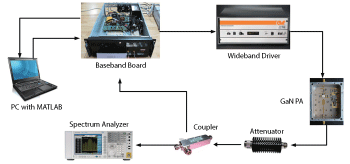
Figure 6 Linearization test setup.
CW Measurements
The PA is biased with Vds = 28 V and the quiescent drain current set at at 120 mA (Vgs = -3.2 V). The results of simulation versus small-signal measurement are shown in the measurements of S11 and S21 (see the lower curves in Figure 5). The measurements are carried out with a vector network analyzer. Gains of 12.1 to 16 dB in the measured band of 1.6 to 3.1 GHz are achieved with a maximum 10 dB return loss. This agrees closely with simulation.
Large signal measurement is carried out with a Keysight E4426B signal generator and E4445A spectrum analyzer. The upper curves in Figure 5 show power at saturation greater than 42 dBm from 1.7 to 2.9 GHz, with the efficiency between 55 and 70 percent.
Modulated-Signal Measurements
The single-ended PA is excited by a 100 MHz bandwidth modulated LTE-Advanced signal with a 7.5 dB peak-to-average power ratio and linearized at 1.95, 2.15 and 2.55 GHz. The test setup is shown in Figure 6. Measured average output power, efficiency and ACLR, with and without DPD, in three frequency bands are summarized in Table 3.
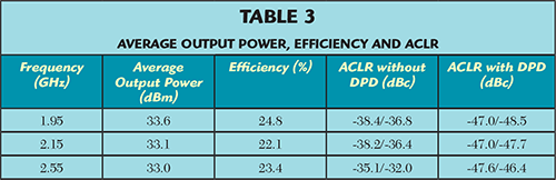
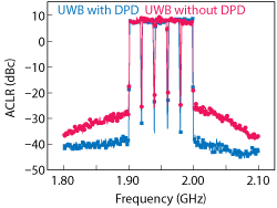
Figure 7 Output spectrum of a 100 MHz LTE-A signal at 1.95 GHz, showing the effect of DPD linearization.
An isolator or 3 dB attenuator is inserted in the front of the PA to reduce the impact of input reflection on DPD. The measured spectra of the PA with and without the DPD for an average 33 dBm output power at 1.95 GHz is plotted in Figure 7. From Table 2, this PA should provide excellent ACLR performance in the three bands.
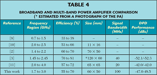
Table 4 compares several broadband and multiband power amplifiers. This compact PA has the smallest structure, excellent efficiency and high linearity.
Conclusion
A compact broadband power amplifier is designed with harmonic control based on the SRFT methodology. A single-ended PA is simulated, designed and measured over 1.7 to 3 GHz. Experimental results show good agreement with simulation. This modified SRFT strategy facilitates PA design, and the resulting amplifier’s compact size provides advantages for many applications.
References
- V. Carrubba, J. Lees, J. Benedikt, P. J. Tasker and S. C. Cripps, “A Novel Highly Efficient Broadband Continuous Class-F RFPA Delivering 74 Percent Average Efficiency for an Octave Bandwidth,” IEEE MTT-S International Microwave Symposium Digest, June 2011, pp. 124.
- P. Wright, J. Lees, J. Benedikt, P. J. Tasker and S. C. Cripps, “A Methodology for Realizing High Efficiency Class-J in a Linear and Broadband PA,” IEEE Transactions on Microwave Theory and Techniques, Vol. 57, No. 12, December 2009, pp. 319623204.
- N. Tuffy, L. Guan, A. Zhu and T. Brazil, “A SimplifiedBroadband Design Methodology for Linearized High-Efficiency Continuous Class-F Power Amplifiers,”IEEE Transactions on Microwave Theory and Techniques, Vol. 60, No. 6, June 2012, pp. 195221963.
- P. Wright, J. Lees, P. J. Tasker, J. Benedikt and S. C. Cripps, “An Efficient,Linear, Broadband Class-J-Mode PA Realized Using RF Waveform Engineering,” IEEE MTT-S International Microwave Symposium Digest, June 2009, pp. 6532656.
- J.H. Kim, S.J. Lee, B.H. Park, S.H. Jang, J.H. Jung and C.S. Park, “Analysis of High-Efficiency Power AmplifierUsing Second Harmonic Manipulation: Inverse Class-F/J Amplifiers,”IEEE Transactions on Microwave Theory and Techniques, Vol. 59, No. 8, August 2011, pp. 202422036.
- B.S. Yarman, “Design of Ultra Wideband Antenna Matching Networks via Simplified Real Frequency Technique,” 1st edition, Springer, Germany, 2008.
- B.S. Yarman, “Design of Ultra Wideband Power Transfer Networks,” 1st edition, Wiley, Hoboken, N.J., 2010.
- K.L. Chen and D. Peroulis, “Design of Broadband High-Efficiency Power Amplifier Using In-Band Class-F-1/F Mode-Transferring Technique,” IEEE MTT-S International Microwave Symposium Digest, June 2012, pp. 123.
- S. Azam, R. Jonsson and Q.Wahab, “Designing, Fabrication and Characterization of Power Amplifiers Based on 10-Watt SiC MESFET and GaN HEMT at Microwave Frequencies,” Proceedings of the 38th European Microwave Conference, October 2008, pp. 4442447.
- M. van der Heijden, M. Acar and J. Vromans, “A Compact 12-Watt High-Efficiency 2.1–2.7 GHz Class-E GaN HEMT Power Amplifier for Base Stations,” IEEE MTT-S International Microwave Symposium Digest, June 2009, pp. 6572660.
- P. Saad, C. Fager, H. Cao, H. Zirath and K. Andersson, “Design of a Highly Efficient 2–4 GHz Octave Bandwidth GaN-HEMT Power Amplifier,”IEEE Transactions on Microwave Theory and Techniques, Vol. 58, No. 7, July 2010, pp. 167721685.