
It is projected that in 2019, global data demand will grow to 24.3 exabytes (1 billion gigabytes) per month from the present 2.5 exabytes per month with 97 percent of this growth due to smart mobile devices. An average smartphone user currently uses 800 MB/month and this is projected to rise to roughly 4000 MB/month in 2019.1 With the growing number of apps, cloud computing, video streaming and other bandwidth consuming services the demand for mobile data services will continue to grow rapidly.
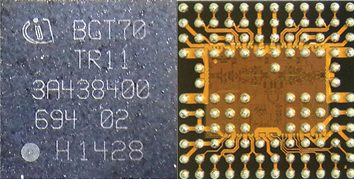
Figure 1 Package view (left and right) of the 71 to 76 GHz transceiver.
Even though mobile devices are getting faster by incorporating new technologies like LTE-Advanced, to provide good quality-of-service (availability, fast speed, connectivity) at reasonable prices to the end customers the network operators also need the backhaul networks which have low latency, much higher capacity and lower total cost of ownership.
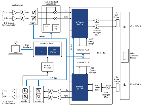
Figure 2 Block diagram of the E-Band front-end module.
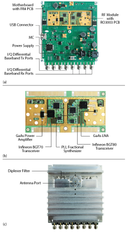
Figure 3 E-Band front-end module evaluation board (a) RF module (b) diplexer filter and antenna port (c).
Optical Fiber is preferred for backhaul because of the high capacity and scalability it can provide but the total cost of ownership (TCO) is quite high. Sometimes it is not feasible to install the fiber in urban areas; longer deployment time, expensive leases and the required approvals from the relevant authorities often make this solution unattractive to carriers.
Microwave radios connect more than 60 percent of all the base stations today but their capacity has been pushed to the limits by using higher modulations, wider channels, polarization multiplexing techniques and radio link bonding.2 The limited channel bandwidth of up to 56 MHz will not be sufficient in future to provide multi-Gbps capacity for the backhaul and fronthaul. On the other hand, in E-Band there is 10 GHz of spectrum available, where even simple modulation schemes can be implemented to achieve several Gbps capacity.
E-Band has worldwide availability, is lightly licensed, interference free, has much wider channel bandwidths (250 MHz and above) available and also low oxygen absorption, allowing much longer hops. Wireless links can be deployed quite quickly compared to optical fiber and also now the technology exists that makes the total cost of ownership of the point-to-point radio link lower than optical fiber. A number of IC manufacturers have developed chip sets for E-Band transceivers, some in silicon and others in GaAs. This article discusses the radio link design and performance that can be achieved at E-Band with a front-end design using Infineon SiGe transceivers.
E-Band Transceivers
E-Band transceivers which can be used for multi-Gbps point-to-point radio links have been developed in SiGe technology. High capacity macrocell backhaul, small cell backhaul, fiber extension or replacement, common public radio interface (CPRI) interconnection are some of the applications which are addressed by the E-Band links. Figure 1 shows an E-Band transceiver for the 71 to 76 GHz band.
In this example, the transceiver chip is fully differential and features a direct up and down-conversion architecture for the Tx/Rx chain. The transmitter, depending upon frequency, can deliver up to +14 dBm saturated output power. The receiver has a double sideband noise figure of 8 dB for the 71 to 76 GHz band.
The transmitter includes a single sideband modulator, a variable gain amplifier and a power amplifier. The transceiver is controlled with a serial peripheral interface (SPI), which can be used to set the variable gain amplifier (VGA) gain in the Tx chain, calibrate the carrier leakage at the Tx output, read the integrated power and temperature sensor. The transceiver can be used in both time division duplex (TDD) and frequency division duplex (FDD) systems. The chip can be switched between Tx and Rx modes in under 1 µs via SPI to enable it to be used in TDD mode. The internal VCO of the transceiver has phase noise better than -80 dBc/Hz at 100 kHz offset from the carrier, which enables radio links with complex modulation schemes to work even in narrower channels to achieve greater than 1.3 Gbps capacity with 256-QAM in the 250 MHz radio channel.
SiGe bipolar technology offers excellent flicker noise performance in comparison to CMOS based technologies, which enables the realization of oscillators with high purity outputs. This in turn helps to achieve higher order modulation schemes and also excellent receiver noise figures at lower IF frequencies. The E-Band transceivers require only single supply voltage of 3.3 V and consume 1.5 W in Tx mode and 1.2 W in Rx mode.
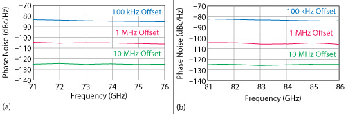
Figure 4 Phase noise performance across 71 to 76 GHz (a) and 81 to 86 GHz (b).
E-Band Front-End Modules
Based on these mmWave transceivers, front-end modules (FEM) have been designed which could be used for radio links with greater than 1 km long hops and over 3 Gbps data rates. The block diagram of an E-Band FEM is shown in Figure 2. In order to cover a longer range (> 1 km) with higher order modulation schemes (up to 256-QAM) using this reference design, a packaged power amplifier (PA) is used at the output of the Tx chain. The saturated output power at the antenna port can be as high as +21 dBm. This topology provides sufficient power at the antenna port to account for the back-off for higher order modulation schemes, the transition losses on board and the losses in the diplexer, as well as having the required fading margin.
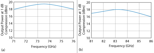
Figure 5 Output power at 1 dB compression across 71 to 76 GHz (a) and 81 to 86 GHz (b).
On the receiver side, an external variable low noise amplifier (LNA) is placed before the E-Band transceiver in order to increase the system sensitivity. The receiver section features automatic gain control circuitry with two stages of external VGA. These are used to deliver a constant level IF signal to the modem even in the case of variations in the received signal at the antenna port. The dual channel differential VGAs are able to cover around 2 GHz of baseband bandwidth. A micro-controller is used to control the E-Band transceiver and the on board PLLs via SPI interface.
For E-Band transceivers, it sets the Tx/Rx mode, Tx VGA control, LO leakage calibration, reading chip ID, reading power and temperature detector, real time Rx AGC. For the PLLs it is used to set the center frequency, charge pump current and reference oscillator offset. An interactive graphical user interface allows the user to control various settings of the E-Band transceiver and PLL via USB connection.
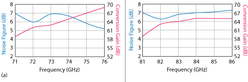
Figure 6 Double sideband noise figure and conversion gain across 71 to 76 GHz (a) and 81 to 86 GHz (b).
Evaluation Board for E-Band Front-End Module
The RF circuitry of the FEM is implemented on a substrate (Rogers RO3003) that was chosen because of relatively low losses at 71 to 86 GHz, lower coefficient of thermal expansion (CTE) in the XYZ plane and low tensile modulus, and the rest of the baseband and control circuitry is designed on an FR4 board. The FEM has an SMA interface for the differential I/Q baseband signals, which allow easy interfacing with an external modem. The diplexer is mounted into the heat sink beneath the motherboard. The evaluation board is powered from an external +12 V supply. The step down converter and low dropout voltage regulator are used to convert +12 V into lower voltages required by various blocks on the evaluation board. The top and bottom views of the FEM are shown in Figures 3a through 3c.

Figure 7 I/Q constellation of a 3.18 Gbps link using 256-QAM with a 500 MHz channel bandwidth at 83.5 GHz. The SNR is 33.5 dB.
Transmit Chain
The chipset integrates an on-chip voltage-controlled oscillator whose output frequency is controlled by an external PLL circuit available on the module. The E-Band transceivers have an internal divider; divide-by 32, which provide the RF signal to the external PLL. An onboard crystal is used to provide the reference signal to the PLL. A fractional PLL is used to lock the carrier to the specific channel in a band. The measured phase noise at the antenna port of the FEM is shown in Figures 4a and 4b.
The baseband bandwidth for the E-Band transceiver is specified to be 1 GHz, which translates into RF bandwidth of 2 GHz. The IF levels fed into the Tx chain of the FEM can be adjusted by the VGA in the IF Tx chain or to some extent by the modem itself. The E-Band transceivers have an internal DAC at the transmitter side to suppress the LO leakage at the Tx port. The onboard microcontroller runs the algorithms, which are used to do LO leakage calibration. External DC biasing at the modulator inputs of the E-Band transceivers allow further suppression of the LO leakage for higher order modulation schemes.
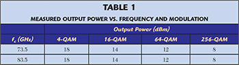
In order to have a higher capacity link for longer hops the output of the E-Band transceiver is fed into two external packaged GaAs power amplifiers. A low loss microstrip to waveguide (WR12) transition is designed at the output of power amplifiers to feed the signal to the diplexer. The integrated diplexer on the module has low insertion loss (under 0.5 dB) and higher isolation (greater than 70 dB) in order to prevent any kind of desensitization of the receive chain. The output P1dB, measured at the antenna port, for the 71 to 76 GHz and the 81 to 86 GHz band is shown in Figures 5a and 5b. Table 1 lists the measured output power at the antenna port with different modulation schemes in channel bandwidth of 500 MHz.

Figure 8 I/Q constellation of a 1.37 Gbps link using 256-QAM with a 250 MHz channel bandwidth at 83.5 GHz. The SNR is 36 dB.
Receiver Chain
On the Rx side an LNA is placed before the E-Band transceiver in order to improve system sensitivity for higher order modulation schemes (> 64-QAM). A low-loss waveguide-to-microstrip transition and balun are used to convert the single-ended output of the LNA to the differential interface of the E-Band transceiver on the board. The differential IF output of the E-Band transceiver is connected to the automatic gain control chain consisting of the external VGAs and power detector. The measured noise figure and conversion gain of the receiver at the antenna port across frequencies is shown in Figures 6a and 6b.
The FEM is currently able to achieve up to 256-QAM in the 500 MHz channel bandwidth, providing a data rate of 3.18 Gbps in a bi-directional link. The measured 256-QAM constellation for this FDD link operating at 83.5 GHz is shown in Figure 7. The link is working with a signal-to-noise ratio (SNR) of greater than 33 dB for the bidirectional link.
The data rate is limited in this demo due to the limited symbol rate from the baseband generator. The E-Band transceivers are specified to work up to 2 GHz RF bandwidth. A modem capable of delivering higher symbol rates (> 500 Msymbols/s) can provide higher capacity radio links but with lower order modulation schemes, e.g., 32 or 64-QAM.
Using much wider channel bandwidth will increase the integrated noise in the band thus reducing the SNR required to sustain higher order modulations (> 32-QAM). As an example, comparing the measured SNR for the 83.5 GHz link operating in the 250 MHz RF channel bandwidth from Figure 8 with the SNR of the link from Figure 7, it can be seen that doubling of the RF channel bandwidth reduces the SNR by 2.5 dB.
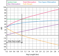
Figure 9 Fade margin vs. hop length for a 256-QAM signal at 83.5 GHz with 500 MHz channel bandwidth and +8 dBm power at the antenna port.
For the E-Band FEM, link distance simulations are performed for 99.99 percent link availability. A vertically polarized antenna with 43 dBi of gain is considered, per the minimum antenna gain requirements of the FCC. The ITU-R P.837-6 K-region rain model with rain rate of 42 mm/h exceeded for 0.01 percent of the average year is considered for this simulation. The fade margin is calculated from the following equations:
- System Gain (dB) = Transmit Power - Receiver Threshold Power for BER of 10-6
- Total Attenuation (dB) = Free Space Attenuation + Attenuation Due to Rain and O2
- Fade Margin (dB) = System Gain - Total Attenuation
The measured receiver threshold for a BER of 10-6 is -50 dBm for 256-QAM in a 500 MHz RF channel bandwidth. Using the above equations, Figure 9 shows a hop length of 1 km is achieved for a 3.18 Gbps radio link. Under similar conditions, the link operating with 64-QAM will cover 1.3 km and 4-QAM will cover 2.4 km.
Conclusion
The E-Band FEM reference design is able to achieve a 3.18 Gbps radio link using 256-QAM in a 500 MHz RF channel bandwidth with +8 dBm of output power at the antenna port. The module is able to cover 1 km with standard antennas using 256-QAM and even longer distances with lower order modulation. The FEM is an all-SMT solution offering excellent performance in a compact form factor with a flexible interface, which can easily be used with an external modem.
ACKNOWLEDGMENT
The author would like to thank the RF team at
GreenWaves S.r.L. for their inputs on the E-Band front-end module.
References
- Cisco Visual Networking Index: Global Mobile Data Traffic Forecast Update 2014-2019 Whitepaper, www.cisco.com/c/en/us/solutions/collateral/service-provider/visual-networking-index-vni/white_paper_c11-520862.html.
- J. Hansryd and J. Edstam, “Microwave Capacity Evolution,” Ericsson Review, 01/2011.