
The use of antenna resonance for characterizing the dielectric constant of an FR-4 substrate is demonstrated. The maximum error in predicting the resonant frequency of a patch antenna by this method is found to be three percent while minimum error is 0.3 percent. This is within the range of typical impedance control (10 percent) provided by PCB manufacturers. A step-by-step guideline and formula are provided. This approach is inexpensive and involves the straight-forward measurement of return loss.
For the design of planar RF and microwave circuits there are many dielectric substrates that can be chosen depending on applications and cost factors. In a commercial environment, cost is a major determinant; hence FR-4 glass epoxy laminate is often used. It is one of the most inexpensive substrate materials and is familiar to many PCB designers. A major issue, however, is the lack of accurate dielectric constant information for FR-4 at RF and microwave frequencies. Datasheets provided by various manufactures provide εr at just 1 or 10 MHz, making it necessary for circuit designers to further characterize the material before using it in their designs.
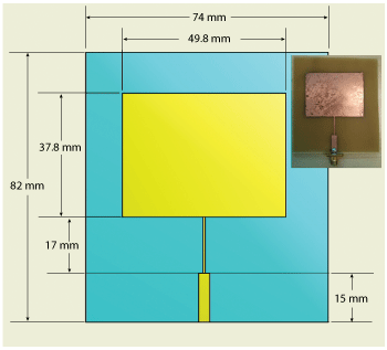
Figure 1 Simulated dimensions and photograph of the fabricated first-pass antenna.
PCB manufactures can control the impedance of specified traces to keep them within desired tolerances; however, impedance control is done using TDR measurements at 1 or 10 MHz. The instrumentation is not capable of performing TDR measurements at higher frequencies such as 2.5 or 5 GHz used for Wi-Fi applications.1 There are other dielectric characterization methods such as free space transmission/reflection measurement systems,2 test circuits based on parallel-coupled microstrip resonators,3 the utilization of transmission information with optimization algorithms,4 the use of loaded microstrip antennas,5 ring-resonator techniques,6 capacitance and S-parameter techniques,7 and the use of impedance analyzers.8 Although any of these methods can be used to characterize the permittivity of dielectric substrates at a desired frequency, they all require specialized measurement equipment and, in some cases, a sample of PCB substrate material. The ring-resonator technique described by Rashidian et al.,6 and the time-domain method of Fidanboylu et al.,9 use trial and error to arrive at approximate values, making them more complex to use.
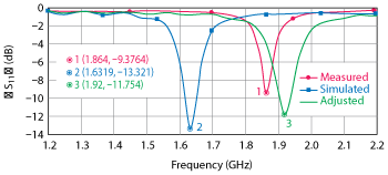
Figure 2 First-pass antenna results.
This article describes a simplified method using a step-by-step procedure and formula to derive the dielectric constant from the measured resonant frequency of a patch antenna. The method and formula are experimentally verified. This requires fabrication of a microstrip antenna at the desired operating frequency. We use 3G and Wi-Fi as examples and hence two patch antennas are designed. This is a one-time characterization process and does not require further validation unless a new PCB substrate is used or greater accuracy is desired.
WORKFLOW
The first step is to design a simple microstrip patch antenna on FR-4 substrate using values of dielectric constant and loss tangent provided in the material datasheet (i.e., at 10 MHz). Resonant frequencies of measured and simulated antennas are then compared. Because the fabrication parameters (i.e., dimensions) are the same as the simulated design parameters, the shift in resonant frequency is assumed to be due to differences between the measured and simulated dielectric constants. From this information, a new dielectric constant is determined and used in a second pass of simulation and design. The second pass serves as a validation and an input for determining the dielectric constant at a new frequency.
FR-4 is characterized at 3G and Wi-Fi frequencies, 1.9 and 2.5 GHz, respectively. Two passes of simulation and fabrication are performed. Three data points are then used to extrapolate the value of the dielectric constant over the frequency range.
EXTRACTED PARAMETER CALCULATION
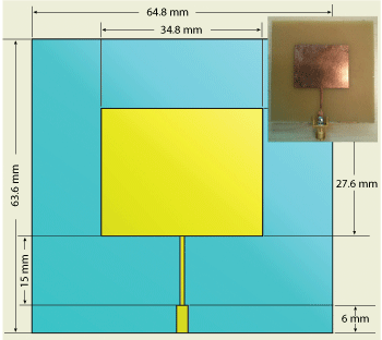
Figure 3 Simulated dimensions and photograph of the fabricated second-pass antenna design.
By rearranging the microstrip patch antenna equations,10 the following is obtained for relative permittivity or dielectric constant.
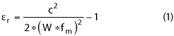
where W is the width of the patch, fm is the center frequency and c is the speed of light.
This must be corrected for the fringing effect of the antenna with air above the patch. To remove the fringing effect, Equation 1 is offset by a fringing factor as shown in Equation 2.
where h is the thickness of the substrate.
ANTENNA SIMULATION AND MEASUREMENT
Computer Simulation Technology (CST) software is used for the design and simulation of the patch antenna. The first step is to calculate the antenna length and width using traditional analysis. Simulation is performed to verify the calculated resonant frequency. The microstrip patch antenna is fed by a microstrip line and quarter wavelength matching is used to match the antenna impedance to 50 Ω. Fine tuning is required to perfectly match the antenna impedance and hence some recursive simulation is performed. The simulated model is then fabricated on FR-4.
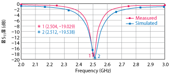
Figure 4 Second-pass antenna results.
Figure 1 shows the simulated dimensions and the fabricated first-pass antenna using a dielectric constant of 4.6 at 10 MHz, per the datasheet. The simulation (see Figure 2) predicts resonance at 1.63 GHz. The difference in resonant frequency between measurement (1.864 GHz) and simulation is clearly apparent. Since all parameters except the dielectric constant are the same, the conclusion is that the resonant frequency difference of 232 MHz is caused by the use of an incorrect dielectric constant in the simulation. Through the application of Equations 1 and 2, the dielectric constant at 1.864 GHz is found to be 3.25.
The adjusted result shown in Figure 2 is determined by repeating the simulation using the same antenna dimensions but with the calculated dielectric constant. The new simulation now predicts resonance at 1.92 GHz (56 MHz higher than measured). This indicates that the dielectric constant of the substrate material is closer to 3.25 than it is to the value 4.6 that is stated within the datasheet.
For validation, a second simulation is performed at 2.5 GHz. Using the calculated dielectric constant of 3.25, the patch antenna is redesigned to resonate at 2.5 GHz (see Figure 3). Figure 4 compares measured and simulated results for the second pass. The resonant frequency of the simulated patch antenna is 2.504 GHz, whereas the fabricated antenna resonates at 2.512 GHz – a difference of only 8 MHz.
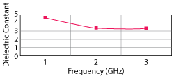
Figure 5 Extrapolation of dielectric constant vs. frequency.
Using three data points for the dielectric constant, an extrapolation (see Figure 5) provides predicted values derived from measurement over the frequency range of interest.
CONCLUSION
A resonant frequency method is used to measure the dielectric constant of PCB laminate material. This is useful for characterizing inexpensive FR-4 material, such as 1080 and glass epoxy laminate, at microwave frequencies. The experimental result for a single pass yields a difference of 56 MHz in the resonant frequency between simulation and measurement. This is within three percent of the measured resonant frequency using the calculated dielectric constant of 3.25. For a second pass, the difference is further reduced to within 0.3 percent of the measured resonant frequency.
References
- M. N. Afsar, J. R. Birch, R. N. Clarke and G. W. Chantry, “The Measurement of the Properties of Materials,” Proceedings of the IEEE, Vol. 74, No. 1, January 1986, pp. 183−199.
- N. Gagnon, J. Shaker, L. Roy, A. Petosa and P. Berini, “Low-Cost Free-Space Measurement of Dielectric Constant at Ka Band,” IEEE Proceedings on Microwaves, Antennas and Propagation, Vol. 151, No. 3, June 2004, pp. 271−276.
- E. L. Holzman, “Wideband Measurement of the Dielectric Constant of an FR-4 Substrate Using a Parallel-Coupled Microstrip Resonator,” IEEE Transactions on Microwave Theory and Techniques, Vol. 54, No. 7, July 2006, pp. 3127−3130.
- J. A. Hejase, P. R. Paladhi and P. Chahal, “Terahertz Characterization of Dielectric Substrates for Component Design and Nondestructive Evaluation of Packages,” IEEE Transactions on Components, Packaging and Manufacturing Technology, Vol. 1, No. 11, November 2011, pp. 1685−1694.
- K. Borah and N. S. Bhattacharyya, “Magneto-Dielectric Material with Nano Ferrite Inclusion for Microstrip Antennas: Dielectric Characterization,” IEEE Transactions on Dielectrics and Electrical Insulation, Vol. 17, No. 6, December 2010, pp. 1676−1681.
- A. Rashidian, M. T. Aligodarz and D. M. Klymyshyn, “Dielectric Characterization of Materials Using a Modified Microstrip Ring Resonator Technique,” IEEE Transactions on Dielectrics and Electrical Insulation, Vol. 19, No. 4, August 2012, pp. 1392−1399.
- C. Wenbin, K. G. McCarthy, A. Mathewson, M. Copuroglu, S. O’Brien and R. Winfield, “Capacitance and S-Parameter Techniques for Dielectric Characterization With Application to High-k PMNT Thin-Film Layers,” IEEE Transactions on Electron Devices, Vol. 59, No. 6, June 2012, pp. 1723−1729.
- Z. M. Dang, J. W. Zha, Y. Yu, T. Zhou, H. T. Song and S. T Li, “Microstructure and Dielectric Characterization of Micro-Nanosize Co-Filled Composite Films with High Dielectric Permittivity,” IEEE Transactions on Dielectrics and Electrical Insulation, Vol. 18, No. 5. October 2011, pp. 1518−1525.
- K. M. Fidanboylu, S. M. Riad and A. Elshabini-Riad, “A New Time-Domain Approach for Determining the Complex Permittivity Using Stripline Geometry,” IEEE Transactions on Instrumentation and Measurement, Vol. 39, No. 6, December 1990, pp. 940−944.
- R. Garg, “Microstrip Antenna Design Handbook,” Artech House, Norwood, Mass., 2001.