
A new W-Band balanced quadrupler using a 0.1 µm GaAs PHEMT process is designed and tested. Measured results show the output power is approximately 3 to 8 dBm from 80 to 95 GHz. The low conversion loss (CL) balanced quadrupler uses a pair of antiparallel Schottky diodes and a pair of input/output amplifiers. Open stubs are employed to match the diode impedance for low CL and a detailed harmonic analysis is given to describe the stub-loading mechanism. The input/output amplifiers are used to reduce the influence of the quadrupler’s external impedance.
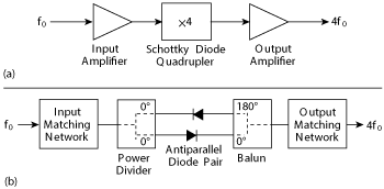
Figure 1 Block diagram of the multiplier (a). Balanced Schottky diode quadrupler (b).
W-Band signal sources are of interest for various applications such as radiometer, automotive radar, foreign object debris (FOD) detection and test instrumentation. Frequency multiplication is the popular approach for generating these signals in the microwave and millimeter wave bands, and Schottky diodes are commonly used. Compared with high frequency oscillators, this is a good approach for realizing a stable, low noise frequency source;1 however, it is not easy to achieve high-efficiency multiplication, especially with an increasing working frequency.
There has been much research applied to improving the multiplier’s performance. Yongshik Lee et al.,2 designed high-efficiency W-Band GaAs monolithic frequency multipliers based on low loss finite ground coplanar lines. Seng-Woon Chen et al.,3 analyzed and designed a high-performance MMIC doubler. A shorted stub was used to short the second harmonic frequency at the input and an open stub was used to short the fundamental frequency at the output, but there was no detailed explanation of how the open and shorted stubs’ impacted CL. Thomas et al.,4 later analyzed the effects of harmonic terminating impedances on CL. Thomas and Branner5 and Johnson et al.,6 used similar design approaches in their active multiplier designs.
It is difficult to directly apply these methods, since the multiplier in this article is not single-ended, but a balanced multiplier that includes a pair of anti-parallel diodes and a balun. Since CL is a strong function the of the multiplication factor, it is more appropriate to use harmonic analysis for the low CL quadrupler design – an approach that has rarely been reported. In this work, a W-Band low CL MMIC quadrupler is designed using harmonic analysis and electronic design automation (EDA) technology. Prototype measurements agree closely with design predictions.
W-BAND QUADRUPLER DESIGN
Figure 1a shows a block diagram of the multiplier. It consists of three parts: input amplifier, Schottky diode quadrupler and output amplifier. Input and output amplifiers allow the Schottky diode quadrupler to work more stably because it is not easily affected by other (input and output) circuits. Figure 1b shows a block diagram of the balanced Schottky diode quadrupler using an anti-parallel diode pair. Here, only the even harmonic frequencies can be obtained at the output.
Balanced Schottky Diode Quadrupler8,9
Schottky diode nonlinear characteristics are depicted by


Figure 2 Quadrupler schematic.
where is is the reverse saturation current, V is the diode external voltage, and α is the diode slope parameter (α ≈ 38 V-l for typical high-quality gallium arsenide Schottky barrier diodes). Figure 2 shows the quadrupler schematic.
In the multiplier mode, the fourth harmonic is generated by multiplication of the reflected second harmonic.
When V = Vf0cosωf0t, iL can be expressed as

where I2k(αVf0) is the modified Bessel function of the second kind, and k is an integer. The load current iL contains a DC term and even harmonics. With an increasing value of k, the even harmonic coefficient gradually decreases. The fourth harmonic is obtained from equation 2 when k=2.
In the mixer mode, the mixing products of reflected even harmonics and the fundamental contain the fourth harmonic. In Figure 2, the total conductance of the anti-parallel diode pair multiplier is expressed as

In microwave and millimeter wave circuits, short or open circuit stubs can be used to reflect harmonics. The fundamental can be viewed as the local oscillator signal (LO), and reflected even harmonics can be considered radio frequency signals (RF) with magnitudes much lower than LO.
In the mixer model with open stubs (MMOS), the voltage of the even harmonic open circuit (OC) transmission line is

where V+ is the voltage amplitude of electromagnetic wave propagating along the positive direction, ωs is even harmonic angular velocity, and t is propagation time. The fundamental can be seen as the LO, and reflected even harmonics can be considered RF defined as

Since the RF amplitude is much smaller than the LO, the total conductance of the diodes can be expressed as the conductance of the diodes modulated only by the LO. Substituting equation 5 into equation 3 yields

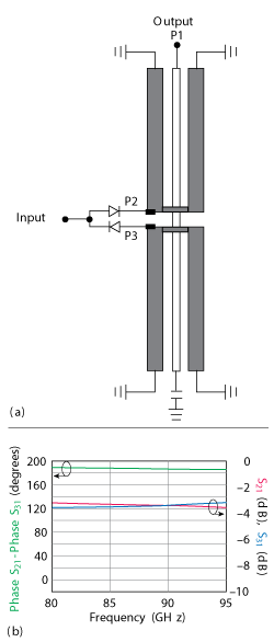
Figure 3 Balun structure (a). Simulated phase and insertion loss (b).
According to Ohm’s law, the output current of the diodes is

This implies that the total current of the anti-parallel diode pair contains only the frequencies (mωf0 + nωfs) where (m + n) is an odd integer. When fs = 2f0, the total current of the antiparallel diode pair contains only frequencies for which (m + 2n) is an odd integer; when fs = 6f0, the total current of the antiparallel diode pair contains only frequencies for which (m + 6n) is an odd integer…and so on. The diodes again generate the fourth harmonic, increasing fourth harmonic output power.
In the mixer model with shorted stubs (MMSS), the voltage of the even harmonic short circuited (SC) transmission line is

And the output current is

Equations 8 and 11 show that the phase of the fourth harmonic produced by the multiplier mode is the same as the fourth harmonic produced by MMOS, but is 90-degrees different than the fourth harmonic produced by MMSS. Consequently, open stubs increase fourth harmonic output power, whereas shorted stubs reduce it. Open stubs are therefore used in the design of the low conversion loss balanced quadrupler.
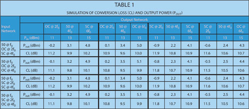
A miniaturized planar balun11 is used in the Schottky diode balanced quadrupler (CSDBQ) structure. The simulated performance of the Marchand balun on GaAs substrate is shown in Figure 3. Only even order harmonics appear at the output port of the balanced multiplier. The input power, fundamental and important harmonics (second, fourth and sixth harmonics) of the CSDBQ are considered. The input and output reflector networks include a 50 Ω matching circuit (50), SC and OC. Some conclusions can be reached from Table 1:
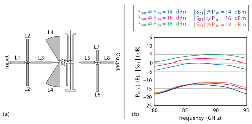
Figure 4 Optimized quadrupler design (a). Simulated output power and |S21| (b).
- The input port harmonic reflector network has little effect on CL.
- Suitable input fundamental power can reduce CL by about 1 dB.
- A second harmonic OC at the output port reduces CL by about 1 dB.
- A sixth harmonic OC at the output port reduces CL by only about 0.2 to 0.4 dB.
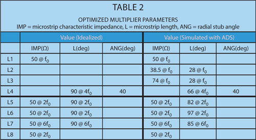
Applying the results from analysis and simulation yields the optimized multiplier structure shown in Figure 4a. ADS-optimized element values are listed in Table 2. Performance is summarized in Figure 4b. Maximum Pout (~ 5 dBm) and minimum CL
(~ 13 dB) occur near 87 GHz when input power is around 18 dBm.
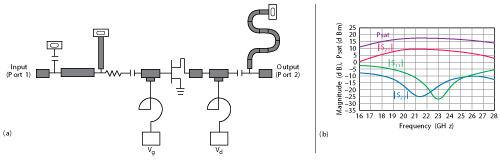
Figure 5 Input amplifier design (a). Simulated performance (b).
Input/Output Amplifier
To reduce the variation of the input/output impedance of the Schottky diode quadrupler. A 4 × 50 µm transistor die is used in the design of the input amplifier and a 2 × 50 µm die is used in the design of the output amplifier. Schematic diagrams and simulated performance are shown in Figures 5 and 6.
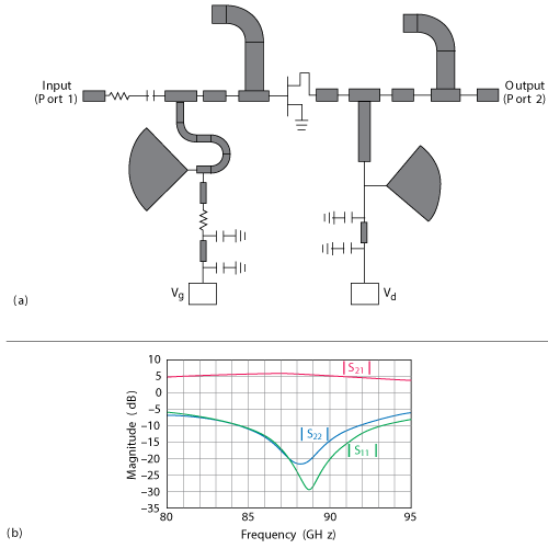
Figure 6 Output amplifier design (a). Simulated performance (b).
QUADRUPLER SIMULATION AND MEASUREMENT
Simulation (see Figure 7), predicts Pout of approximately +4 to 11 dBm from 80 to 95 GHz, and CL of approximately 0 to 7 dB. Output power is maximum when the input power is 14 dBm. When the input power is 8 dBm, CL is a minimum. This is because input amplifier gain compression increases as input power increases.
The quadrupler is fabricated with a 0.1 µm gate-length GaAs PHEMT process. The assembled quadrupler chip (see Figure 8a) is 1 × 3.4 mm. It is tested on-wafer using a Cascade probe station (Cascade M150), W-Band GSG probe (Cascade ACP110-S), and W-Band power probe (Keysight W8486A).
Measured curves are shown in Figure 8b, while Figure 8c compares simulated and measured data. Figure 8c shows a slight shift in output characteristics between simulation and measurement. This is mainly due to the difficulty in obtaining an accurate Schottky diode model at W-Band and the more pronounced impact of dielectric loss and fabrication accuracy with increasing frequency.
Figure 7 Full quadrupler design (a). Simulated output power and S21 performance (b).
CONCLUSION
A W-Band balanced quadrupler is analyzed, designed and tested. Harmonic analysis and EDA technology are used to optimize the circuit and reduce CL. Open stubs are employed to match the diode impedance for low CL. In order to reduce the influence of the multiplier’s external impedance, amplifiers are placed at the input and output. Finally, a small sized MMIC quadrupler is manufactured with using a 0.1 µm gate-length GaAs PHEMT process. Its output power is approximately 3 to 8 dBm from 80 to 95 GHz.
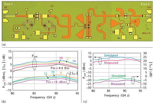
Figure 8 Fabricated quadrupler (a). Measured output power and S21 (b). Comparison of simulated and measured performance with 12 dBm input (c).
References
- Y. Campos-Roca, L. Verweyen, M. Fernández-Barciela, E. Sánchez, M. C. Currás-Francos, W. Bronner, A. Hälsmann and M. Schlechtweg, “An Optimized 25.5–76.5 GHz PHEMT-Based Coplanar Frequency Tripler,” IEEE Microwave and Guided Wave Letters, Vol. 10, No. 6, June 2000, pp. 242–244.
- Y. Lee, J. R. East and L. P. B. Katehi, “High-Efficiency E-Band GaAs Monolithic Frequency Multipliers,” IEEE Transactions on Microwave Theory and Techniques, Vol. 52, No. 2, February 2004, pp. 529–535.
- S. Chen, T. C. Ho, K. Pande and P. D. Rice, “Rigorous Analysis and Design of a High-Performance 94 GHz MMIC Doubler,” IEEE Transactions on Microwave Theory and Techniques, Vol. 41, No. 12, December 1993, pp. 2317–2322.
- D. G. Thomas Jr. and G. R. Branner, “Optimization of Active Microwave Frequency Multiplier Performance Utilizing Harmonic,” IEEE Transactions on Microwave Theory and Techniques, Vol. 44, No. 12, December 1996, pp. 2617–2644.
- D. G. Thomas Jr. and G. R. Branner, “Single-Ended HEMT Multiplier Design Using Reflector Networks,” IEEE Transactions on Microwave Theory and Techniques, Vol. 49, No. 5, May 2001, pp. 990–994.
- J. E. Johnson, G. R. Branner and J. P. Mima, “Design and Optimization of Large Conversion Gain Active Microwave Frequency Triplers,” IEEE Microwave and Wireless Components Letters, Vol. 15, No. 7, July 2005, pp. 457–459.
- D. M. Kang, J. Y. Hong, J. Y. Shim, J. H. Lee, H. S. Yoon and K. H. Lee, “A 77 GHz mHEMT MMIC Chip Set for Automotive Radar Systems,” ETRI Journal, Vol. 27, No. 2, April 2005, pp. 133–139.
- M. Cohn, J. E. Degenford and B. A. Newman, “Harmonic Mixing with an Antiparallel Diode Pair,” IEEE Transactions on Microwave Theory and Techniques, Vol. MTT-23, No. 8, August 1975, pp. 667-673.
- T. Yang and X. J. Huang, “Design of Ka-Band Doubler,” International Journal of Infrared and Millimeter Waves, Vol. 22, No. 12, December 2001, pp. 1825–1829.
- Y. Fang, B. Zeng, T. Gan, H. Zhang and Y. Yuan, “Quadrupler Cuts Losses at W-Band,” Microwaves & RF, June 2014.
- W. M. Fathelbab and M. B. Steer, “New Classes of Miniaturized Planar Marchand Baluns,” IEEE Transactions on Microwave Theory and Techniques, Vol. 53, No. 4, April 2005, pp. 1211–1220.