
This article reviews the basics of fully-differential amplifiers (FDA), important specifications and what they mean, and how to interface to the signal chain using an FDA for balun-type functionality with additional performance.
In today’s world, most high-speed analog-to-digital converters (ADC) have differential inputs. These ADCs are used in a wide variety of applications ranging from, but not limited to, communications wireless infrastructure and backhaul to test and measurement oscilloscopes and spectrum analyzers. To support this input architecture, engineers must design the signal chain to interface to the ADC differentially.
It is easy to assume that one must use a balun in the signal chain for best performance, despite coupling issues in some applications. This is not always the case, however, especially in test and measurements where the DC component is needed. Fully differential amplifiers (FDA) are versatile tools to use in place of (or along with) baluns and offer a variety of benefits. Fully differential signal processing provided by FDAs gives the circuit design increased immunity to external noise, twice the dynamic range and reduced even-order harmonics versus traditional amplifiers with single-ended outputs.
What is an FDA?
Imagine not having the luxury of an FDA integrated circuit (IC) to drive a differential ADC. One approach, other than a balun, is to create a differential signal using two operational amplifiers, one providing the positive (Vin+) and the other providing the negative (Vin-) input signal. To establish the proper external gain, eight resistors are needed.
With half the resistor count and only one IC, an FDA can provide both a single-ended-to-differential-interface and a differential-to-differential interface to the ADC. This also eliminates the need for a balun and allows DC components to pass; a balun provides DC isolation. This is important in many applications that need a superior response at low frequencies down to DC. An FDA is two amplifiers in one, a main differential amplifier (from Vin to Vout) composed of multiple feedback paths and the Vocm error amplifier (better known as the common-mode output amplifier).
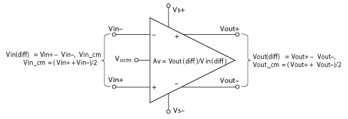
Figure 1 Diagram of a typical fully-differential amplifier.
The Vocm amplifier samples the differential voltage (Vout+ and Vout-) internally and compares it to the voltage applied to the Vocm pin. Through an internal feedback loop, the Vocm amplifier is used to drive the “error” voltage of the Vocm error amplifier (the voltage between the input pins) to zero, so that Vout_cm = Vocm (see Figure 1). If the Vocm pin is left floating, the bias point usually defaults to Vcc/2 (midway between supplies) through an internal voltage divider. This Vocm setting on the (Vocm) pin can impact the overall output swing (as discussed later). This is different than in a traditional op amp with a single-ended output, where the output common-mode voltage and single-ended output are inherently the same signal, impacting the dynamic range.
In addition to the Vocm error amplifier, the main differential amplifier in the FDA has both a Vout+ and Vout- output and multiple feedback paths. When analyzing this amplifier it is best to think of it as including two inverting feedback paths. One consists of an inverting input to non-inverting output, and the other is a non-inverting input to an inverting output (see Figure 1). For the FDA to function properly, both paths must be closed. To maintain balance, the feedback paths are best kept equal. Analysis of these two paths can become very complicated. The analysis is simplified in this discussion to introduce FDA basics and illustrate how they can assist design. FDA input and output voltages are defined in Figure 1.

Figure 2 Basic FDA gain configuration, differential input-to-differential output.
In Figure 2 external resistors are added to the basic FDA diagram to set the gain. For this simplified analysis, we define β1 and β2 as the feedback terms.

The full Vout (diff) equation in terms of feedback, Vin+, Vin- and Vocm is

Equation 3 shows that if the feedback terms are not equal, the differential output voltage depends on Vocm. This is important, because the feedback terms should be equal or as close to each other as possible, because the Vocm term introduces both an offset and noise. With Vocm = 0, the gain becomes

FDA Benefits
Inherent in its differential architecture, the FDA improves noise immunity and system dynamic range. System noise can accumulate and impact dynamic range when signals travel across a printed circuit board (PCB), cables and wiring, and through signal and ground paths. The FDA enables coupled noise to be rejected at the inputs. This includes noise from power supplies and signals that appear as a common-mode in a typical op amp. Single-ended components cannot reject ground noise as each part has a different reference point. Despite diligent design efforts to control high-frequency ground currents, issues may arise where differential signaling can improve performance. Noise accumulation in a typical op amp may degrade signal-to-noise ratio (SNR), compromising system design.
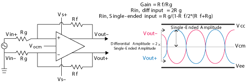
Figure 3 Dynamic range increase in FDAs.
Along with greater noise immunity due to common-mode rejection by the FDA, the phase difference between the outputs enables the output voltage swing to be twice that (6 dB) of a single-ended output (see Figure 3). This increases the amplifier’s headroom using the same power supply or allows the use of a lower voltage power supply, with lower dissipation, for the same signal swing.

Figure 4 Fully differential amplifier configuration.
A further advantage of FDAs and differential signal chains is inherent cancellation of even-order harmonics. Using a power series expansion, given a sine wave input and ignoring the DC component, Figure 4 illustrates second-order harmonic cancellation in nonlinear differential devices such as amplifiers (FDA). While full cancellation cannot be achieved in real devices, these products see a benefit from a balanced design over a single-ended configuration (see Figure 5).

Figure 5 Single-ended amplifier configuration.
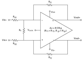
Figure 6 FDA with additional Rt to adjust noise gain.
FDAs also provide excellent output balance critical to driving differential ADCs. Phase and amplitude components of the signal into the ADC are ideally matched for best performance. When there is unbalance in either or both the amplitude and phase, this is seen as a common-mode component on the output, producing SNR degradation. An ideal FDA can provide precisely 180° phase difference between the Vout+ and Vout- signals. Since the internal common-mode feedback circuitry forces the output common mode to equal the applied common mode at the Vocm, the balance error, Equation 5, is minimal.

Specifications
Of the specifications that may be of particular interest in high-speed system designs, linearity should be well understood; items that may need to be reviewed are common-mode voltage, noise and stability.
Common-Mode Voltage Range
It may seem obvious how specifying the common mode voltage range impacts performance; however, a review of this topic is helpful since this is what makes the FDA so powerful. When choosing an FDA to drive a device such as an ADC, it is important to consider the differential ADC’s common mode voltage and how this aligns with the FDA’s common mode voltage range as well as Vout peak-to-peak (Vpp (out)) capability. For AC-coupled signals, Vocm alignment with the ADC is not much of a concern as long as the input and output range are within specifications and are supplied as needed. Usually, one can default to mid supply of the amplifier to achieve best performance. An important consideration is Vpp (out) to meet maximum signal swing of the ADC. For an optimal system design, including margin to accommodate loss in the anti-aliasing filter is good design practice. For example, if the full scale ADC input is 1.2 Vpp and there is a 2 dB anti-aliasing filter loss, ideally 1.5 Vpp or higher should be available at the amplifier output to provide the needed margin.
In a DC-coupled design, knowing both the required Vocm and voltage swing is paramount. Use Equations 6 and 7 to check that the amplifier can meet the desired output swing around Vocm.

With a DC-coupled signal, the performance and common-mode specifications at the desired Vocm must be verified. Typically in an FDA datasheet, Vicm and Vocm specifications are noted with minimum and maximum values. Additionally, graphs are provided to show the linearity impact and optimal range for the FDA common-mode voltage.
Depending upon the FDA, power supplies may sometimes be aligned to maintain a Vocm just outside an optimal range for alignment with the ADC. Consider, for example, an FDA with ideal performance specified at mid-supply with ±0.5 V of range and an ADC at 1.5 V Vocm. The supply to be used is a split supply, such that the amplifier is at Vs(+) = +4 V and Vs(-) = -1 V. Once verified that the required swing can be accommodated and that these supplies meet datasheet specifications, there should be no issue in using them to satisfy output common mode voltage needs.
Noise and Stability
Noise gain (NG) is essential to determining output noise and stability. Different from signal gain, noise gain is the reciprocal of the attenuation from the output of an amplifier (or any feedback loop) to the input and is equal to

Assuming Rf1 = Rf2 and Rg1 = Rg2 in Figure 2, the noise gain is 1/β1 or 1/β2. Keep in mind that sometimes gain bandwidth products (GBP) are specified for FDAs. This is also dependent on NG as GBP (Hz) is equal to bandwidth in Hz times NG.
For simplicity, we assume purely resistive feedback. Capacitors added to the feedback and input can impact stability and NG, making the NG expression with complex impedance equal to

Note the difference in the noise gain, Equation 8, and the signal gain, Equation 4. Their independence allows noise gain to be manipulated with signal gain held constant. For simplicity, only resistive feedback is considered in the following example. In Figure 6, a signal gain of 2 is desired in the FDA, but this FDA is stable only for NG ≥ 3. For stability at this lower gain value, a ‘dummy’ resistor is added at the input (Rt in the differential configuration). The parallel combination of Rs and Rt is used to manipulate the amplifier’s noise gain, while Rg and Rf are the signal gain-setting resistors. Adding Rt adjusts the noise gain for stability. By manipulating the noise gain with Rt, the amplifier is stabilized without impacting the signal gain or signal bandwidth. With increased NG, however, the system should be evaluated to determine if its impact on SNR and increased sensitivity to input offset voltage can be tolerated.
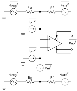
Figure 7 FDA noise analysis simplified.
What is its impact on noise? To determine that, it helps to review the steps for evaluating the use of an FDA as a differential ADC driver. The SNR of an n-bit ADC is quantified in Equation 10. For simplicity, assume that the ADC’s SNR is the same as the reciprocal of total harmonic distortion (SINAD) and noise of the ADC. Given this, we can use the effective number of bits (ENOB) to calculate if the output noise of our FDA is sufficient to drive our ADC.

To calculate the FDA output noise, first reduce the circuit under evaluation to its simplest form (see Figure 7). Assume that the resistors are balanced and match as close as possible on each side. This ensures the balance of the FDA and match for the maximum HD2, IMD2 performance. Also assume that the total differential noise is the root sum of the squares (RSS) of the individual contributors (see Equation 11).

Where:
NG = 1_?
eni = input voltage noise
(specified in datasheet of FDA)

in = input current noise
(specified in datasheet of FDA)
k = Boltzman’s constant
(1.38 × 10⁻²³j/°K)
T = absolute temperature (273°K)
Having determined the output noise, will this work in the system? For the anti-aliasing filter, we use a third order lowpass filter (N=1, ENB=1.57×BW; N=2, ENB=1.22×BW; N=3, N=1.15×BW; and so on). This means that the system noise bandwidth is 1.15×BW (signal). From here we use Equations 12-14 to check compatibility:

Finally, compare the one LSB value, which is in Vpp, to the output noise of the filter+FDA Vpp. If this is comparable, it is time to build an evaluation board to verify the calculation and assumptions. Note that the number ‘6’ used in Equation 13 is based on the assumption of a Gaussian noise distribution.
Single-Ended Input Applications
What if you have a single-ended input and need to convert for a differential ADC? Most would say this is exactly what baluns were made to do. However, these devices cannot provide a power gain, are susceptible to coupling by design, over temperature specifications are typically not well maintained, can be very big and costly if wideband signals are needed, and do not preserve the DC component. In a high speed system such as a communications receiver chain used in a test and measurement spectrum analyzer or oscilloscope, preserving the DC component while enabling GHz frequency capability may be necessary. In this case, an FDA can be a very useful tool.
If the design is DC-coupled, ensure both sides of the input circuit are configured to retain balance. The non-signal input side typically has an Rg component biased to the midrange of the expected source. This mid-scale reference point should give a balanced differential swing around Vocm at the output. This is generally grounded if the source swings around ground. Configuring the FDA gain with external resistors provides design flexibility. Selected feedback resistors should be equal. Additionally, the impedances on each side from the summing junctions back to both the signal source and ground (or bias voltage, non-signal side) should be equal. Solve for Rt, Rg1 and Rg2; for detailed analysis refer to the LMH5401 datasheet.1
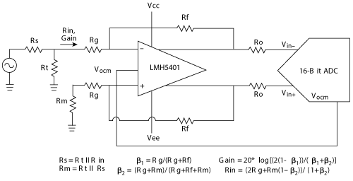
Figure 8 DC-coupled, single-ended input, differential output.
Figure 8 shows a final schematic of the high-speed FDA using a 50 Ω source impedance (Rs) and G = 4 V/V. The NG in this example is established by NG1=1+Rf1/Rg2, or just over three, which is unconditionally stable for this FDA.
CONCLUSION
While this article covers only the basics of fully differential amplifiers, hopefully the information will help influence your choice of amplifier by informing you of options. Before reaching for the balun, ask yourself if an FDA is more appropriate.
References
- LMH5401 datasheet, January 2015, www.ti.com/lit/ds/symlink/lmh5401.pdf?DCMP=lmh5401&HQS=hpa-hsp-amp-contrib-070-lmh5401-pf-en.
- B. Razavi, “RF Microelectronics,” Upper Saddle River, N.J.: Prentice Hall, 1998.
- P.R. Gray and R.G. Meyer, “Analysis and Design of Analog Integrated Circuits,” Fourth Edition. New York: Wiley, 2001.
- J. Karki, “Using Fully Differential Op Amps as Attenuators, Part 1: Differential Bipolar Input Signals,” Texas Instruments Analog Applications Journal, 2nd Qtr. 2009, pp. 33–36.
- J. Karki, “Using Fully Differential Op Amps as Attenuators, Part 3: Single-Ended Unipolar Input Signals,” Texas Instruments Analog Applications Journal, 4th Qtr. 2009, pp. 19–22.
Carissa Sipp is the RF systems applications engineer for TI’s high speed group. She received her bachelor’s degree from The Ohio State University in Columbus, Ohio. Carissa can be reached at ti_csipp@list.ti.com.