
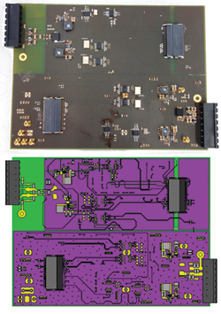
Figure 1 Manufactured demonstrator board (top) and the equivalent simulation model (bottom).
EMC compliance is a necessary condition for releasing products to market. National and international standards bodies such as the IEC2 and the FCC3 define limits on the emissions a device is allowed to produce, and automotive and aerospace manufacturers can set even stricter standards for their OEM suppliers. If these standards are not met, the product cannot be sold.
EMC engineering has traditionally been the domain of measurement alone, with the result that EMC compliance was only considered late in the design process, since it required a working prototype. Correcting EMC problems at this late stage can be cost-intensive, especially if multiple prototype iterations are required.
In addition, although measurement can help identify the symptoms of EMC issues, it is only of limited use for identifying the root causes of the problems. This means EMC troubleshooting using measurement is often limited to applying countermeasures such as filters and additional shielding, which can increase the size and the cost of the product, instead of tackling the problem at its source.
Simulation allows EMC compliance to be analyzed earlier in the design process, and in greater depth than is possible with measurement alone. Because simulation doesn’t require a physical prototype, it can be used to investigate many different configurations and answer fundamental “what if?” questions about the design. Decisions that are made early in the design process – for example, the arrangement of the components within the device – are usually difficult to change later on and can be crucial for the EMC compliance of a device.
Simulation is also helpful at the troubleshooting stage, where it is a complementary tool to measurement. Current and field visualization can serve to highlight the locations of EMC problems. They offer more insight into the behavior of the device than a blip on a spectrum analyzer graph can provide, although the measurement is still critical for the final decision as to whether the device passes or fails the test.
This article considers how to test and develop the EMC workflow for modern electronic devices. The demonstrator board (see Figure 1) is based on modern electronic designs, and the principles outlined here are applicable to a wide range of devices. On this board, the power is routed through an input filter to a voltage regulator module (VRM) that drives a power delivery network (PDN) on the PCB. A number of single ended and differential drivers are placed on the board. Some of them are routed over a connector and all of them are finally terminated on the board.
The demonstrator board contains two versions of the same system on a common substrate – one designed to offer good EMC performance (the upper half of the board in Figure 1, called the “good” layout), and one designed to offer poorer performance (the lower half, called the “bad” layout).
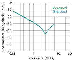
Figure 2 Measured and simulated S-parameters for the input filter, used to extract the parasitic values of the filter.
The components were selected so the board has noise sources in various frequency bands: the VRM is typically driven at a few hundred kHz up to low MHz, the single ended nets typically emit from a few tens of MHz up to 1 GHz, while the frequencies on the differential nets can go as high as 6 GHz.
Simulation Workflow
The first step of electronic layout is to define the logic of the board by sketching out a circuit schematic. However, it is not always possible to estimate the EMC performance just from the schematic, especially when considering radiated emissions instead of conducted emissions. The EMC performance of a device depends not only on its circuit-level representation, but also on the distribution of the capacitors, the routing of the nets and the interactions between signal lines and components. Only a 3D simulation can reveal these effects.
This means that circuit-level simulation methods coupled to full-wave 3D EM simulation can complement each other. These can be combined in a number of different ways: for example, a ‘Combine Results’ task, based on the superposition principle, can be used to calculate the field distribution when a circuit is attached to a 3D model without having to resimulate the entire 3D model, while true transient/EM co-simulation can be used to integrate circuits, including nonlinear components, into a full-wave 3D simulation.
The first step is to define the model geometry and import CAD and EDA data for PCBs and enclosures. Lumped elements, ports, probes and field monitors are also defined at this stage. The ports are what will later provide the link between the full-wave simulation and the circuit simulation. Once these are set up, the simulation can begin.
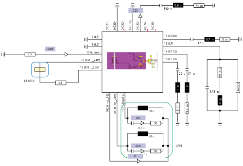
Figure 3 Circuit for a conducted emissions test setup. The simulation block is the large square in the center.
Full wave solvers can be broadly divided into time domain and frequency domain methods. For conducted emissions, where the frequency range is narrow and the fields are confined to the electrically small board, the frequency domain solver is usually the best choice. A frequency domain direct solver only requires one pass to simulate all the ports, which is useful for densely populated boards.

Figure 4 Comparison of simulation and measurement for conducted emissions for a one-capacitor filter (top) and a two-capacitor filter (bottom).
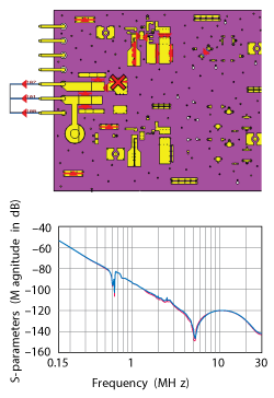
Figure 5 The location of the capacitors under investigation (top). The conducted emissions from the 'good' PCB (bottom), with (red) and without (blue) the highlighted capacitors.
For radiated emissions, a time domain method is a better fit. The time domain solver needs to simulate each port separately, but it can simulate a broad band of frequencies at once, and is more efficient than the frequency domain technique for electrically large simulations.
Regardless of which simulation method is used, the results are the same: the S-parameters of the model and the field distribution inside it. These S-parameters can be used to produce a circuit-level model of the component, which can be incorporated into the schematic of the device.
Circuit solvers are much faster than 3D solvers and, for a simple circuit, a spectrum can be calculated within seconds. This means that the circuit elements can be adjusted interactively, and optimization of the circuit can be carried out in a reasonable length of time. This is especially useful for extracting equivalent circuits for elements and for helping simulation and measurement agree more closely.
In order to match the simulation and measurement, the parasitic values of the mounted elements must be known. To allow the input filter to be simulated accurately, an equivalent circuit is added to the simulation model representing the parasitics inherent in the test fixtures. By using the ‘Tune’ function, the values of the parasitics are varied until the simulation’s behavior matches the measurement. These values are then applied across multiple simulations, while maintaining good agreement between measurement and results (see Figure 2).
Conducted Emissions
Two parts of the system are involved in conducted emissions: the input filter and the voltage regulator. For the analysis presented here, a constant load of 2.5 Ω is placed on the board. This load leads to a high current, so the emission is also quite high. This is, therefore, a worst case set-up.
The conducted emission will be measured using ports at the connector that are connected on the other side to an electric boundary, acting as a virtual reference. This electric boundary creates a low-impedance path for the return current. It is not an ideal external ground, as this cannot exist in a 3D model.
As already discussed, the frequency domain solver is a good choice for most conducted emissions simulations due to the narrow band nature of the signals. In this case the finite element method (FEM) based solver in CST STUDIO SUITE®4 is used to generate the S-parameters. Once the 3D simulation has been run and a schematic block produced, the rest of the circuit can be added (see Figure 3). This means a source representing the LT8610 VRM5, derived from a functional simulation using the manufacturer’s LTSpice tool, and a line impedance stabilization network (LISN) as specified in the CISPR 16 test standard6.
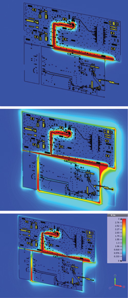
Figure 6 Electric field around the PCB at 100 (top), 350 (center) and 700 MHz (bottom).
The circuit can then be simulated in either the time domain or the frequency domain. Both methods are available regardless of which solver was used for the 3D simulation. Here, an input signal is used which represents the switching effect of the VRM. In this case, a frequency domain method is used, which takes three seconds – extremely fast compared to full-wave simulation.
The results of this frequency domain simulation are shown in Figure 4, calculated between the 0 V input and the protective earth (PE). One capacitor is used in the filter for the first simulation (shown on the top), while in the second simulation (shown on the bottom), a capacitor is inserted into the 24 V branch. The second capacitor improves the emission for the 24 V connection (not shown) but worsens the emission level for the 0 V branch (shown on the bottom). Even where there are discrepancies between simulation and measurement due to the noise-floor of the measurements, simulation offers an excellent prediction of the trends within the data. The increase in the maximum value and the position of the peak are both calculated by the simulation.
Replacing the switching noise with a broadband excitation also makes it possible to assess the performance of the filters and optimize their construction. Since each additional component carries a small cost in terms of money and production time, identifying components which do not contribute to the EMC performance of a device is beneficial. In the simulation in Figure 5, one set of capacitors at the input is found to have virtually no effect on the emissions from the PCB and can be safely removed. Because of the speed of the circuit simulation, dozens of components can be investigated within a few minutes.
Radiated Emissions
For radiated emissions simulations, a different approach is needed. Here, it is usually the field values within the 3D model that are of interest, rather than the voltages at the ports, so field monitors and probes should be defined in areas of interest. A time domain solver is a good choice here, given the broadband nature of the radiated emissions (in this case, 30 MHz to 1 GHz). In this example, the emissions from a trace on the ‘good’ PCB were analyzed using the finite integration technique (FIT) transient solver. The trace runs close to the edge of the reference plane, which means it is a likely candidate for producing radiated emissions.
Again, only one full-wave simulation needs to be carried out. After the field values have been calculated once, the ‘Combine Results’ task can calculate the change in the fields for arbitrary changes to the excitation and termination.
The ability to visualize fields allows engineers to identify the structures and modes which are responsible for the emissions. Figure 6 shows the emissions from the trace at three different frequencies. At the lowest frequency, the field is confined to the trace and the radiation is very low. At 350 MHz, however, there is a resonance in the power-ground system of the PCB, and this mode radiates a significant amount of energy. There is a second peak in the emissions at 700 MHz corresponding to a higher order mode, with the bottom layers oscillating in antiphase.
Once the sources of radiated emissions have been identified, the layout can be modified to attempt to mitigate them. In this case, we move the trace a few millimeters away from the edge of the reference plane. As shown in Figure 7, this successfully reduces the emissions in the vertical direction, but has less impact on emissions in the horizontal direction. This suggests that additional countermeasures may be needed, such as shielding.
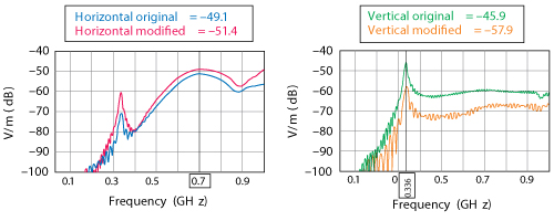
Figure 7 Electric field values 3 m from the PCB showing the reduction in emissions in the horizontal (top) and vertical (bottom) directions when the trace is moved.
In many EMC test chambers, the floor acts as a ground plane and can reflect signals. This can have a significant effect on the measured emissions, as shown in Figure 8, and should be taken into account by the simulation. Including the PCB, with all its fine details, directly in a full-scale model of an anechoic chamber would result in a large simulation domain with an extremely dense mesh. The simulation can be much more efficient if it is a two-step process.
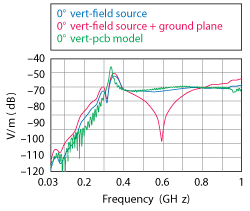
Figure 8 The E field values at 3 m from the PCB. The red line shows the impact of the floor on the detected emissions.
The first step is to simulate the PCB in a small simulation domain with a “field source monitor” surrounding it. The field source monitor records the tangential E and H fields around the PCB and outputs them as a near-field source file. This near-field source is then imported into a second simulation of the anechoic chamber, using a much coarser mesh. According to Huygens’ Principle, the second simulation will create the same radiated emissions as the full 3D model, and it only requires a few minutes. The same approach can be used for modeling other structures which can affect emissions, such as the housing of a PCB.
Conclusion
Simulation is a useful tool for the EMC analysis of complex electronics and allows engineers to identify possible EMC problems early in the design process. Simulation can identify trends which are subsequently confirmed by the measurements. Broadband simulations, in particular, are fast and straightforward and can provide useful data even in cases where the complexity of the measurements makes a direct comparison between simulation and measurement difficult.
References
- Festo, www.festo.com
- IEC/TR EN 61000, Electromagnetic Compatibility (EMC)
- Code of Federal Regulations, Title 47, Part 15 (47 CFR 15), Federal Communications Commission (FCC)
- CST STUDIO SUITE, https://www.cst.com
- LT8610: 42 V, 2.5 A Synchronous Step-Down Regulator with 2.5 µA Quiescent Current, http://www.linear.com/product/LT8610
- CISPR 16, Specification for radio disturbance and immunity measuring apparatus and methods
Andreas Barchanski is the EMC market development manager at CST. He holds an M.Sc. degree in physics and a Ph.D. in numerical electromagnetics from the Technical University Darmstadt. He joined CST as an application engineer in 2007. Besides EMC, his main interest lies in the simulation of various electronic systems ranging from high speed digital to power electronics.
Jens Krämer is the EMC simulation and testing manager at Festo, a leading world-wide supplier of automation technology and a leader in industrial training and education programs. He holds a diploma in electronics from the University Stuttgart. His main interest lies in energy propagation on PCBs and through connectors – both intentional and unintentional.
Pietro Luzzi is an EMC consultant at Festo. He holds a bachelor’s degree in electrical engineering. In 2012 he joined the EMC Simulation & Testing department, where he plans circuit boards and simulates a variety of interactions between EMC and the PCB.