
An Active Physical Device Simulator
HP Eesof
Santa Rosa, CA
Circuit designers have enjoyed the benefits of sophisticated simulation tools for some time. However, these simulation programs are limited to circuit optimization and characterization and are forced to describe the active device by means of established or measured equivalent models. Hence, the circuit is optimized for the application but the device is not.
To achieve optimum total circuit performance, a new simulator system now provides the circuit designer with the ability to vary the physical parameters for the active device. The HP Active Physical Device Simulator (HP APDS) is a design environment and interface to the Leeds Physical Model (LPM) for MESFETs and high electron mobility transistors. The University of Leeds, UK has joined in the effort to integrate the LPM into the HP simulation environment. As a result, the active device’s description is entered into the HP APDS suite using the program’s user-friendly interface and the simulation is performed. Prior knowledge of device physics and numerical analysis is not required.
The HP APDS simulator provides fast and accurate device simulation for III-V compound devices. Simulation results are achieved within minutes rather than hours or days. By incorporating device simulation into the circuit simulation environment, the program permits the use of simulated device data or a model to simulate circuit performance. For example, the device’s recess structure can be adjusted to improve the circuit’s power-added efficiency. The program also can generate large-signal models of devices for use in circuit designs and perform statistical analysis to improve device yields.
Features
Among the features of the HP APDS is its ability to perform ultra-fast quasi-two-dimensional physical device simulation with great accuracy. The simulator takes into account device self-heating, hot electron/velocity overshoot effects, avalanche and gate breakdown. The program includes quantum mechanical effects and predicts DC and high frequency device performance. C-V response and mobility profiles are simulated, along with ungated I-V, DC I-V and S parameters, and physics-based device parasitics can be calculated. In addition, a built-in design of experiments (DOE) is incorporated for device design, as well as an easy-to-use interface.
Applications
HP APDS version 1.0 provides insight into device operation for problem solving, such as determining why a device breaks down. The program also allows true interactive device simulation, permitting the operator to see the influence of physical parameters on electrical performance such as gate length on ft and fmax. The sensitivity of electrical characteristics to variations in physical parameters, such as SWR vs. recess depth, also can be seen. The built-in yield-driven capability improves yield and produces higher quality products, reducing development time and manufacturing cost.
Operation
A new device is created by entering the device geometric information, doping density and specifications for active layers from a device menu. Either planar or single- or double-recessed structures can be selected. The device cross-section parameters, such as ohmic contact width and separation, recess parameters, or gate length and position between the ohmic contacts, can be adjusted. During the process, the device’s parasitics are calculated automatically.
Four types of simulations at process-level analysis provide insight for refining processes: channel profile, mobility profile, C-V and ungated simulations.  Channel profile simulation, shown in Figure 1 , provides carrier density, a conduction band profile and the Eigen spectrum of sub-band energy levels and probability distributions vs. depth (from the device surface or gate). The mobility profile simulation predicts electron mobility vs. etch depth. The C-V simulation produces capacitance vs. voltage characteristics, providing insight to the active-layer design and gate location. The ungated simulation considers the link between recess depth and etch current. In addition, a doping profile is displayed.
Three types of simulation are available at the device level. The device’s DC I-V characteristics at different drain voltages are displayed, and device breakdown is taken into account. Other electrical characteristics, such as potential, electric field, electron energy and velocity, device cross section and sheet carrier density vs. channel length at different bias levels, also are displayed at device profile simulation. This information is helpful for analyzing device operation and assists in design troubleshooting. S-parameter simulation focuses on circuit design. The simulator is able to determine S parameters quickly and easily. Once the 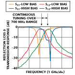 device’s bias is selected, the two-port S parameters and extracted equivalent-circuit element values are displayed in seconds. Parameters such as ?h21?2 and ft and fmax can be displayed, as well as maximum unilateral gain, stable gain and available gain vs. frequency. The resulting equivalent circuit then can be used directly for circuit design. Figure 2 shows a typical S-parameter display.
 At circuit-level simulation, an accurate large-signal device model is necessary for designing power circuits. HP APDS generates such a model with ease and the result can be used directly in power circuit designs. Figure 3 shows an example of how device geometry influences circuit performance or how device doping density affects circuit power-added efficiency.
HP APDS aids in device design optimization by performing DOE simulation. The impact of process variation on device performance can be observed using the DOE dialog. A choice of DC, 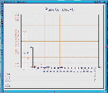 S-parameter or equivalent-circuit analysis completes the entry requirements for DOE. By setting the nominal value and factor variation for each physical parameter to be examined, the nominal device specification and its variation can be determined. DOE results then can be displayed graphically, as shown in Figure 4 , to determine which parameter influences the specific electrical characteristics most strongly.
System Requirements
HP APDS is supported by HP 9000 series 700, Sun SPARC and IBM RS 6000 workstations. Operating systems include HP-UX 10.x, 9.03 or 9.05; SunOS V 4.1.3x or 5.4; Solaris 1.1.1x or 2.4; and AIX 3.2.5 or 4.1 with X/Motif. The FLEXlm license management system is used. Both network and node-locked licenses are available for operation on multiple workstations or a single workstation.
The HP 85290A APDS suite includes design environment, data display, DOE, LPM and APDS UI. Two-day on-site service is provided.
HP EEsof,
Santa Rosa, CA
(800) 452-4844.