
A wideband common-gate (CG) and common-source (CS) CMOS balun-LNA with noise cancellation uses cross-coupled feedback between the CG input transistor and the cascode transistor of the CS input stage to increase LNA input transconductance. Fabricated using a 0.13 µm RF CMOS process, the LNA achieves a flat voltage gain of 18 dB, a NF of 2.7 to 3.2 dB, and an IIP3 of -4.5 to -7.4 dBm over a 3 dB band from 0.1 to 4.4 GHz. It consumes only 4.1 mA from a 1 V supply and occupies an area of 520 × 490 µm2. This LNA has the merits of lower power consumption and lower supply voltage when compared to other reported wideband LNAs. It has comparable gain with negligible additional NF degradation.
With the wide variety of communication protocols in use today such as digital TV, WiMax and Bluetooth, a software-defined radio (SDR) accommodating multiple radio standards is more desirable than ever before.1 This has motivated an increasing interest in wideband receiver techniques.2
The design of a key building block in a wideband receiving front end, the low noise amplifier (LNA), involves a compromise of noise figure (NF), bandwidth and power consumption. Two commonly adopted CMOS wideband LNA topologies are the capacitance cross-coupled (CCC) LNA3 and the common-gate (CG) and common-source (CS) LNA.4 The CCC LNA, however, requires an off-chip balun for single to differential input conversion. For wideband operation, an off-chip passive balun typically has high loss that degrades overall receiver NF.
In most cases, to receive single-ended signals from antennas and drive following differential mixers, a balun-LNA combining the active balun and the LNA into a single circuit becomes a more attractive option.5 This makes the CG-CS LNA with an inherit balun function highly desirable, where wideband input matching, good voltage gain and possibly high linearity can be achieved simultaneously.4,6 Nevertheless, to obtain low NF, a large amount of power must be consumed in its CS stage. This article describes an improved wideband CG-CS balun-LNA with noise cancellation. The CCC technique and bulk effect are adopted to boost the transconductance of the CG stage and the cascode transistor of the CS stage, both of which are beneficial for low noise and low power. Additional noise deterioration ascribed to the two techniques is negligible.
LNA Circuit
Figure 1a shows a conventional CMOS CG-CS LNA consisting of the CG input stage (MCG) and the CS input stage (MCS).4 Thermal noise cancellation for MCG and differential balanced gain can be guaranteed simultaneously by setting gmCGRL1=gmCSRL2, where gmCG and gmCS are the transconductance of MCG and MCS, respectively. To acquire overall low noise, gmCS is often 3 to 5 times gmCG. Consequently, the power consumption of the CS stage always occupies a majority of that of the whole LNA. To alleviate this, an inverting amplifier CS stage including the stacked NMOS and PMOS is used to increase the transconductance of CS stage under fixed power consumption. In addition, a feedback path is added from the drain of MCS to the gate of MCG, boosting the transconductance of MCG and reducing power consumption.6
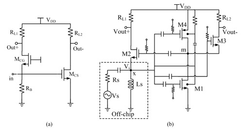
Figure 1 Conventional CG-CS LNA (a) and CG-CS LNA with CCC feedback (b).
Figure 1b shows the design of a CMOS CG-CS LNA, consisting of the CG input stage (M2), the stacked CS input stage (M1?M4), and the cascode stage (M3). The CG input stage achieves the input impedance matching. The cascode M3 is designed mainly to reduce the Miller effect of the parasitic gate-drain overlap capacitance in the stacked CS input transistors. It also helps increase the output impedance and improves input–output isolation. CCC feedback is added between M2 and M3 to boost their transconductance. A bulk couple technique is adopted at the CS input transistors to further enhance effective transconductance. This is beneficial for the low noise and low power of the CS stage. The source choke inductor Ls and the equivalent parasitic capacitance observed at node x, are resonated for input matching to provide an overall low input reflection coefficient within the bandwidth.
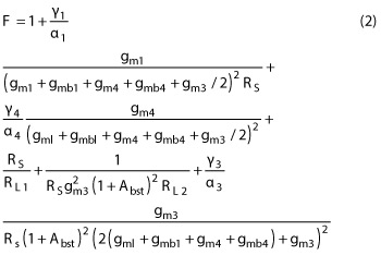
Through small-signal analysis, the voltage gain of the proposed LNA, can be derived as
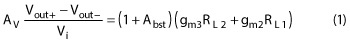
where the gm-boosting coefficient Abst equals (gm1+gmb1+gm4+gmb4)/gm3. Parameters gmi, gmbi, RL1, and RL2 are the gate transconductance and bulk transconductance of FETs and the load resistors of the CG and CS stages. For the balanced differential outputs, the relationship gm3RL2=gm2RL1 must be met. This is also the noise cancellation condition of M2 under the input impedance matching condition Rs=1/gm2(1+Abst). According to Wang et. al.,6 the gain is increased with the bulk effect of CS input transistors being utilized. Due to the feedback path from Vi to the gate of M3, gm3 is also incorporated into equation 1 to further boost the gain of the LNA. Generally, it can be appreciated that the incorporated transconductance of the cascode transistor by the cross-coupled feedback and the bulk effect of the CS input transistors, maintains a comparable transconductance of the CS stage but with reduced bias current. This is the main advantage of the topology.
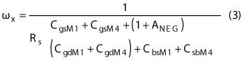
After derivations with the input impedance matching condition, the noise factor expression of the LNA yields:
where α and γ are the bias-dependent parameters. The second and third expressions are from the noise of M1 and M4. The fourth and fifth expressions are from the loads of RL1 and RL2. The last is from M3. Due to the feedback path from Rs to the gate of M3, it is no longer an ideal cascode transistor (i.e., contributing no noise).7 The noise derivation equation 2, however, shows that the noise contribution of M3 is far smaller than that of M1 by a factor of gm3/4gm1(1+Abst)2 (0.01 in the design). Thus, the additional degradation in NF can be negligible. Moreover, compared to that reported by Wang et. al.,6 thanks to the bulk effect of the CS input transistors and gm3 being incorporated into the transconductance of CS stage, the noise of M1 and M4 can still be effectively inhibited but with reduced bias currents.
According to equation 2, as Abst increases, NF decreases; however, with increased frequency things become complex. A large Abst generates a low frequency pole at node m as shown in Figure 1b and introduces an additional phase shift in the CS stage. The differential phase shift between the CG and CS stages has an adverse impact on the noise cancellation of M2, because an ideal cancellation requires that the differential voltages of Vout+ and Vout- have exactly the same magnitudes and opposite phases. In other words, the imbalanced phase shift caused by a large Abst could increase the overall NF and reduce the bandwidth.
Due to large parasitic effects in stacked transistors, the bandwidth of the LNA is limited mainly by the pole in the CS stage signal path. This path must be examined carefully. Using small signal methods to analyze the circuit of Figure 1b, one can determine that the bandwidth at node m is the same as that reported by Wang et. al.6 Meanwhile, for node x, the bandwidth yields:
where CgsM1, CgsM4 ,CgdM1, CgdM4, CbsM1, and CsbM4 are the gate source capacitance, gate drain capacitance, and source bulk capacitance of M1 and M4, respectively. The utilization of the bulk effect, introduces parasitic capacitances CbsM1 and CsbM4, but this does not constitute a limitation since all of these parasitic capacitances can be resonated with off-chip inductor Ls.
Measurement Results
The LNA core circuit is implemented using standard 0.13 µm RF CMOS technology. Figure 2 is a micrograph of the LNA, which occupies 520 x 490 μm2 including the probing pads. With a single 1 V power supply, transistors M1 and M2 are biased at 3.68 and 0.45 mA, respectively, while parameter Abst is taken as 2.5. RL1 and RL2 are set to 250 and 100 ohm, respectively. Two source-follower buffers are added after the outputs of the LNA to drive 50 ohm loads. An external passive balun is also used at the outputs of the buffers for a test target.
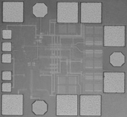
Figure 2 Chip micrograph.
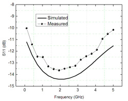
Figure 3 Measured and simulated S11.
Figure 3 shows the measured and simulated input reflection coefficients. Owing to the inherent wideband input match of the common-gate topology, |S11| is below -10 dB across a wide frequency range of 0.1 to 5 GHz. Figure 4 shows |S21|, demonstrating a flat gain of 18 dB over a 3 dB frequency band from 0.1 to 4.4 GHz. Figure 5 compares both the measured and simulated NFs. The measured result shows a maximum noise figure NFmax of 3.2 dB at 4.4 GHz and an average NF of 2.7 dB. Although it is about 0.7 dB higher than the simulated NF, the shape and the flatness of the measured curve are almost the same, which we believe to reflect the actual NF of the LNA. In contrast to the bias current of 5.7 mA, reported by Wang et. al.,6 this is accomplished with a bias current of 4.1 mA due to the incorporated transconductance of the cascode transistor and the bulk effect of the CS input transistors. Gain and noise performance is achieved with comparable CS input transistor transconductance but with reduced bias current.
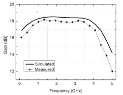
Figure 4 Measured and simulated gain.
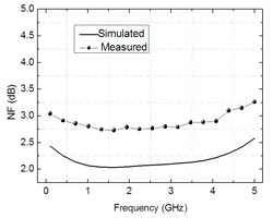
Figure 5 Measured and simulated NF.
The high order distortion generated by M2 is cancelled in accordance with the noise cancellation principle described by Blaakmeer et. al.4 Thus, LNA linearity is dominated mainly by the voltage to current conversion transistors M1 and M4 of the CS input stage. By adjusting the bias and size of M4 to cancel the second-order nonlinearity of M1 with only minor impact on the third-order nonlinearity, an optimized IP3 is achieved.6 The input third-order intercept point (IIP3) of the LNA is measured at 1, 2 and 3 GHz with a two tone of 5 MHz spacing. In Figure 6, the measured IIP3 drops from -4.5 to -7.4 dBm when the frequency is increased from 1 to 3 GHz. This can be ascribed to the fact that as the frequency increases, the distortion cancellation of the LNA is deteriorated by the large phase shift of the CS stage.
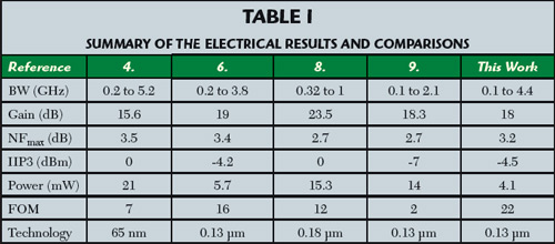
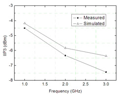
Figure 6 Measured and simulated IIP3 within the band.
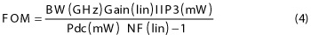
Measured performance of the LNA is summarized in Table 1. Other recently published wideband LNAs are also included for comparison with a figure of merit (FOM) defined by equation 4.10 The LNA achieves comparable NF and gain with lower power consumption, and has the highest FOM among these designs.
Conclusion
An improved wideband noise cancelling balun-LNA in common-gate and common-source topology is described. Cross-coupled feedback and the bulk effect are adopted to increase the input transconductance of the LNA. Gain and noise performance comparable to other reported LNAs are achieved with reduced bias current. Fabricated in a 0.13 µm RF CMOS process, the LNA achieves a flat voltage gain of 18 dB, a NF of 2.7 to 3.2 dB and an IIP3 of -4.5 to -7.4 dB over a 3 dB frequency band from 0.1 to 4.4 GHz. It consumes only 4.1 mA from a 1 V supply, which is quite suitable for low voltage and low power applications.
Acknowledgment
This work was supported by the National Natural Science Foundation of China (No. 60901019).
References
- F.M. Ghannouchi, “Software-Defined Radio Transmitters for Advanced Wireless and Satellite Communications Systems,” Microwave Journal, Vol. 51, No. 5, May 2008, pp. 202-216.
- C.X. Chen, M.A. Do, K.S. Yeo, C.C. Boon and W.M. Lim, “A Low-Power Multi-Channel UWB Single Chip Transceiver With Pulse Detectors,” Microwave Journal, Vol. 55, No. 10, October 2012, pp. 104-122.
- W. Zhuo, X. Li, S. Shekhar, S.H.K Embabi, J.P. de Gyvez, D.J. Allstot and E. Sanchez-Sinencio, “A Capacitor Cross-Coupled Common-Gate Low-Noise Amplifier,” IEEE Transactions on Circuits and Systems II: Express Briefs, Vol. 52, No. 12, December 2005, pp. 875-879.
- S.C. Blaakmeer, E.A.M. Klumperink, D.M.W. Leenaerts and B. Nauta, “Wideband Balun-LNA With Simultaneous Output Balancing, Noise-Canceling and Distortion-Canceling,” IEEE Journal of Solid-State Circuits, Vol. 43, No. 6, June 2008, pp. 1341-1350.
- B. Guoand and G. Wen, “Periodic Time-Varying Noise in Current-Commutating CMOS Mixers,” Progress in Electromagnetic Research, Vol. 117, June 2011, pp. 283-298.
- H. Wang, L. Zhang and Z. Yu, “A Wideband Inductorless LNA With Local Feedback and Noise Cancelling for Low-Power Low-Voltage Applications,” IEEE Transactions on Circuits and Systems I: Regular Papers, Vol. 57, No. 8, August 2010, pp. 1993-2005.
- X. Fan, H. Zhang and E. Sánchez-Sinencio, “A Noise Reduction and Linearity Improvement Technique for a Differential Cascode LNA,” IEEE Journal of Solid-State Circuits, Vol. 43, No. 3, March 2008, pp. 588-599.
- M. Moezzi and M.S. Bakhtiar, “Wideband LNA Using Active Inductor With Multiple Feed-Forward Noise Reduction Paths,” IEEE Transactions on Microwave Theory and Techniques, Vol. 60, No. 4, April 2012, pp. 1069-1078.
- Z. Li, L. Chen, Z. Wang, C. Wu, J. Cao, M. Zhang, C. Wang, Y. Liu and Z. Wang, “Low-Noise and High-Gain Wideband LNA With gm-Boosting Technique,” Electronics Letters, Vol. 49, No. 18, August 2013, pp. 1126-1128.
- H. Zhang, X. Fan and E. Sánchez-Sinencio, “A Low-Power, Linearized, Ultra-Wideband LNA Design Technique,” IEEE Journal of Solid-State Circuits, Vol. 44, No. 2, February 2009, pp. 320-330.