
Near-field Mapping above a Coupled-line Filter and a MMIC
This article presents a comparison of the electric field measured with the modulated scattering technique and calculated with finite-difference time domain (FDTD) simulations for a three-stage coupled-line microstrip bandpass filter. Electrically small dipoles and monopoles 150 and 100 mm long, respectively, are used as modulated scatterers for the measurements. The comparisons are performed at 10 GHz at a mean height of 50 mm above the filter with monolithically integrated Schottky diode probes on 40 mm-thick silicon substrates. The electric field map of the tangential field component (measured and simulated) is displayed with the same scale at 10 GHz. In addition, the normal electric field map of a distributed amplifier is presented using the scattered signal from the output port of the amplifier. The low cost modulated scattering system is capable of mapping the normal and tangential electric field intensities and electrical phase delays above a microwave circuit in the frequency range of 0.5 to 18 GHz with a spatial electric field resolution of better than 100 mm. This article demonstrates that both the FDTD and modulated scattering techniques are powerful developmental tools that can be used together to accurately characterize the behavior of microwave circuits.
Thomas P. Budka
RF Diagnostics
Plano, TX
Emmanouil M. Tentzeris, Scott D. Waclawik, Nihad I. Dib, Linda P.B. Katehi and Gabriel M. Rebeiz
University of Michigan, Electrical Engineering and Computer Science Dept.
Ann Arbor, MI
Most standard testing techniques for characterizing MMICs involve on-wafer probing where the device under test (DUT) is contacted at several ports outside the circuit. S-parameter measurement systems have been demonstrated up to W-band with passive probing techniques1 and remain the most widely used technique for testing microwave circuits. However, during microwave circuit design and development, circuit resonances may occur as part of network analyzer measurements that often go unexplained. Using a map of the electric field intensity and phase above the substrate, a microwave engineer is able to view the internal performance of a microwave circuit directly and thus gain a greater understanding of the circuit's operation. Tighter control over line lengths, coupling and losses may be achieved, thereby saving valuable chip real estate.
Electromagnetic field mapping of microwave circuits is possible with electro-optic sampling,2,3 photo-emission sampling,4 electron-beam sampling,5 scanning force microscopy,6 passive detection schemes7,8 and modulated scattering.9-20 Electro-optic, photo-emission and electron-beam sampling generally are time domain methods, while scanning force microscopy, passive detection and modulated scattering are frequency domain methods. Of all the current electromagnetic near-field detection methods for microwave circuits on any substrate, the easiest and least expensive to implement below 60 GHz is the modulated scattering method. This technique was proposed in the 1950s9-11 and applied to planar microwave circuits at 1.4 to 2.2 GHz.13
In this article, the results of modulated scattering tests over a coupled-line bandpass filter at 10 GHz and a distributed amplifier are presented. The filter field results are compared with calculated results from the FDTD technique.14 By using monolithically integrated monopole and dipole scatterers, the uncorrected true electric field resolution of the system has been pushed to below 100 m m at 10 GHz and the probe's interaction with the microwave circuit has been minimized. The system is capable of characterizing all electric field components over a microwave circuit, and it is believed that the resolution can be pushed to 25 m m with smaller and thinner probes before the system becomes noise limited. The systems developed at the University of Michigan currently operate from 500 MHz to 18 GHz and can be extended for operation up to 60 GHz using a coaxially based system.
The Modulated Scattering System
As part of the basic operation of the modulated scattering system, a small dipole scatterer with a diode mounted at the center is placed in the near field of the circuit of interest. By modulating the bias of the diode at a frequency much lower than the RF, a weak modulated scattered RF signal is returned to the transmitter. By using the input port to the DUT also as a receiving port of the scattered signal, the modulated signal can be detected with little or no distortion of the near electric fields. The strength and phase of the scattered signal are related directly to the square of the normalized electric field distribution intercepted at the position of the dipole or monopole scattering probe.9
In the RF section of the near-field modulated scattering experiment, part of the RF signal is sent as the LO to a wideband quadrature mixer from point 5 to point 6. A modulated scattering probe with a diode mounted or integrated with the electrically small antenna (dipole, monopole or loop) is placed in close proximity to the DUT at a specific position. Because the power scattered to the input/output port by the probe is small (orders of magnitude less than the input power to the DUT), homodyne mixing is used to detect the weakly modulated signal. The reflected scattered signal is diverted to a wideband homodyne quadrature mixer and the in-phase and quadrature IF (10 to 100 kHz) voltages are detected by a lock-in amplifier. The signal levels from the in-phase and quadrature channels of the mixer for a typical microwave circuit with 10 dBm input power range from 10 mV to 10 mV when measured with a lock-in amplifier with a 10 dB gain preamplifier. Through the use of an absorptive RF switch, both the scattered reflected (input port) and scattered transmitted (output port) waves can be detected by the same quadrature mixer.14 A schematic of the RF section of the modulated scattering experiment is shown in Figure 1 .
 The integrated scattering probes are mounted on a computer-controlled submicron translational stage. By moving the probe over a region of interest, a two-dimensional electric field image from the normal and tangential electric fields is collected. The entire system is controlled via a PC and fits on a small table.
Monolithic Probe Design and Fabrication
The design of a probe is critical to the operation of any electric field mapping system. As described previously, hybrid probes on 125 m m quartz wafers were fabricated initially.14 In this article, monolithic probes on a 40 m m-thick high resistivity silicon substrate (0.1 ld at 200 GHz) are used to map the electric fields over microwave circuits. The diodes are highly doped, low capacitance Schottky diodes with resistive bias lines to minimize coupling of the bias lines with the DUT. The series resistance of a single diode is measured at 12 W . The junction and parasitic capacitance (Cj + Cp ) of the dipole diode is 2 pF and results in a cutoff frequency of 40 GHz.
 Figure 2 shows the 150 m m-long integrated dipole and the 100 m m-long integrated monopole used for this research before dicing. Individual probes have an overall length of 5 mm and a width of 0.5 mm. The resistive feeding transmission
 lines are specified to
 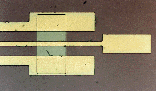 have a characteristic impedance of 120 W and rapidly attenuate any RF signal that may propagate along the bias lines. Figure 3 shows the integrated probe holder with an etched groove for probe self alignment. The probe is on 40 m m-thick silicon mounted on a low resistivity 500 m m-thick silicon wafer with a silver-epoxied low frequency connector on the right.
The Test Filter
 Figure 4 shows the geometry of a three-stage coupled-line filter fabricated on RT/Duroid 6010 (e r = 10.8, h = 0.635 mm) and
 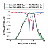 mounted on an open carrier. The bandpass filter has a measured insertion loss of 2 dB in the pass band from 8 to 10.5 GHz and provides better than -25 dB rejection at 12 GHz. Figure 5 shows the measured and FDTD-calculated S parameters of this filter. The small deviation in the S11 results is most likely due to imperfect SMA-to-microstrip transitions at the input and output of the filter beyond 10 GHz.
Application of the FDTD Method
The FDTD method17 is employed for a theoretical analysis of the coupled-line filter. The first step in the process is to define a problem space of reasonable dimensions for computation. In this case, the spacing of the mesh is specified to be 52.9 m m in the vertical direction, 100 m m in the propagation direction and 25 m m in the direction normal to propagation. The time step is specified to be 73 fs to satisfy the Courant stability criterion.14 These specifications produce a structure with 140 x 234 x 448 cells. The first-order Mur's absorbing boundary condition18 is applied to the boundaries of the problem space with superabsorbers19 at the input and output planes.
For wideband S-parameter extraction, a Gaussian pulse of 100 ps is used as the microstrip excitation source. Two simulations of pulse propagation along the microstrip line are made: one for the filter and one for a 50 W microstrip through-line. For the filter simulation, the sum of the incident and reflected waveforms is calculated; for the through-line, the incident waveform is calculated. The reflected waveform at the input port is determined by subtracting the incident waveform of the through-line from the total waveform of the filter. The reflection coefficient S11 is determined by the ratio of the Fourier transforms of the reflected and incident waveforms. The transmission coefficient S21 is determined by the ratio of the Fourier transforms of the transmitted and the incident waveforms. The waveforms are probed at distances far enough from the filter discontinuities to eliminate the effects of evanescent waves.14
For the electric field calculation, sinusoidal waves of 10 GHz for the pass band are used as microstrip excitations. The excitations are vertical and matched to the feedline. (Total impedance of the source region is equal to the characteristic impedance of the feedline (50 W ).) The source is applied five meshes inside the feedline in the propagation direction and the values of the electric fields are calculated during the sixth period of the sinusoidal waveform to avoid the transition-period effect.14
Measurements
Figure 6 shows tangential electric field intensity |E|2 images in the transverse  direction above the three-stage coupled-line filter obtained from modulated scattering measurements and FDTD calculations in the pass band at 10 GHz. The horizontal spacing between measurements is 50 m m and the longitudinal spacing is 250 m m. For this project, a 150 m m-long integrated dipole probe is scanned across an area of 12,250 x 3800 m m over the filter with the dipole oriented transverse to the propagation direction. Over this large scan area, the height of the probe above the filter varies from 20 to 70 m m due to bowing of the substrate and alignment errors. From studies of the decay of the electric field intensity with height, the error introduced by a height misalignment of 50 m m within this range can be, at most, 3 dB in electric field intensity. Tighter alignment is possible with planar semiconductor substrates and with tests over smaller areas.
The results with integrated probes presented in this article show that no spatial averaging is necessary for the dipole measurements and that the electric field data nearly match the true electric field at a simulated height of 100 m m above the coupled-line filter. Due to the extensive amount of time required to run a single FDTD simulation, the electric field response was calculated only at two heights: 0 and 100 m m.
A feature the measurements show that the calculations do not predict is an asymmetric tangential field distribution along a cross section of the input and output microstrip transmission lines. This unexpected effect at 10 GHz does not appear in the tangential electric field measurements at 9, 11 or 12 GHz (measurements not shown) and, therefore, is definitely an actual effect of the circuit. The measurements also show a peak in the field near the center section of the bandpass filter. This section of the filter is potentially radiating and would couple more strongly to a scattering probe than would other regions of the circuit.
Frequency domain movies for this filter were collected between 9 and 12 GHz, but are not presented here. Much like a frequency sweep on a network analyzer, a frequency movie allows an unprecedented view of the complete operation of a microwave circuit. This information can help detect coupling of a specific filter with a nearby device on a MMIC and allow the establishment of experimentally determined design rules or the validation of electromagnetic simulation software.
Distributed Amplifier Measurement
The model TGA8310-SCC distributed amplifier IC used for the measurement is a 2 to 20 GHz nine-transistor amplifier on a 100 m m-thick GaAs substrate.20 The S parameters of the amplifier are measured from 2 to 20 GHz. Over this band, the gain ranges between 5 and 6 dB with a return loss better than 15 dB and S12 between -40 and -25 dB, making a measurement of the scattered reflected wave impractical due to the high level of attenuation from the scattering  points beyond the amplifier to the input port.
The measured normal electric field intensity (grayscale) and phase (contours) of the scattered transmitted signal with the layout of the amplifier's metal layer superimposed over the test region measured with a 100 m m-long integrated monopole is shown in Figure 7 . As the theory predicts, the peak electric field over the input meander line is at approximately the same level as the peak electric field over the output meander line.
In a distributed amplifier, a portion of the incoming RF power is coupled into each transistor, thereby reducing the electric field intensity along the input meander line. Similarly, the electric field strength along the output meander line should increase with intensity as each amplifier stage adds RF power in phase to yield a maximum electric field intensity at the output of the distributed amplifier. The measured peak electric field at the output meander line occurs near the seventh and eighth transistors. The location of this peak has been observed to vary at other frequencies and indicates a small standing wave along the output line. For an ideal distributed amplifier, the phase along the main RF path that is measured with this modulated scattering technique should be constant. The phase contours vary from 65° to 80° over the main RF path indicating nearly ideal operation.
Conclusion
Unlike other electromagnetic field mapping systems, the modulated scattering system has proved to be very flexible for microwave circuits fabricated on any substrate (Duroid, GaAs and quartz). The system is modular with an RF detector system, probes, a translational stage, a frequency source and a lock-in amplifier, and any component may be replaced or improved without affecting the operation of the other system components. These results, as well as other modulated scattering measurements over microwave circuits and antennas, can be viewed on the World Wide Web at http://members.aol.com/rfdiag.
Acknowledgment
The authors wish to thank the NASA/Center for Space Terahertz Technology for its support; Rogers Corp. for its generous donations of RT/Duroid, which was used in numerous microwave test circuits for this research; Texas Instruments Inc. for donating the amplifier; and Steve Nelson and Randy Lehmann of Texas Instruments Inc. for donating several X-band MMICs to the University of Michigan for these tests.
References
1. E.M. Godshalk, "A W-band Wafer Probe," IEEE MTT-S Digest, 1993, pp. 171-174.
2. W. Mertin, C. Bohm, L.J. Balk and E. Kubalek, "Two-dimensional Field Mapping of Amplitude and Phase of Microwave Fields inside a MMIC Using the Direct Electro-optic Technique," IEEE MTT-S Digest, 1994, pp. 1597-1600.
3. G. David, W. Schroeder, D. J?sger and I. Wolff, "2D Electro-optic Probing Combined with Field Theory Based Multimode Wave Amplitude Extraction: A New Approach to On-wafer Measurement," IEEE MTT-S Digest, 1995, pp. 1049-1052.
4. J. Bokor, A.M. Johnson, R.H. Storz and W.M. Simpson, "High Speed Circuit Measurements Using Photoemission Sampling," Applied Physics Letters, Vol. 49, No. 4, July 28, 1986, pp. 226-228.
5. J.T.L. Thong, "Transmit Time Effect in Electron Beam Testing Voltage Measurements," Measurement Science Technology, Vol. 3, 1992, pp. 827-837.
6. C. B?shm, C. Roths and E. Kubalek, "Contactless Electrical Characterization of MMICs by Device Internal Electrical Sampling Scanning-force-microscopy," IEEE MTT-S Digest, 1994, pp. 1605-1608.
7. S.S. Osofsky and S.E. Schwarz, "Design and Performance of a Noncontacting Probe for Measurements of High Frequency Planar Circuits," IEEE Transactions on Microwave Theory and Techniques, Vol. 40, August 1992, pp. 1701-1708.
8. Y. Gao and I. Wolff, "A Miniature Magnetic Field Probe for Measuring Fields in Planar High Frequency Circuits," IEEE MTT-S Digest, 1995, pp. 1159-1162.
9. J.H. Richmond, "A Modulated Scattering Technique for the Measurement of Field Distribution," Institute Radio Eng. Transactions, MTT-3, 1955, pp. 13-15.
10. A.L. Cullen and J.C. Parr, "A New Perturbation Method for Measuring Microwave Fields in Free Space," Proceedings IEE, B 102, 1955, pp. 836-844.
11. R. Justice and V.H. Rumsey, "Measurement of Electric Field Distributions," Institute of Radio Eng. Transactions, AP-3, 1955, pp. 177-180.
12. G. Hygate and J.F. Nye, "Measuring Microwave Fields Directly with an Optically Modulated Scatterer," Measurement Science Technology, Vol. 1, 1990, pp. 703-709.
13. J. Zürcher, "A Near-field Measurement Method Applied to Planar Structures," Microwave Engineering Europe, June/July 1992, pp. 43-51.
14. T.P. Budka and G.M. Rebeiz, "A Microwave Circuit Electric Field Imager," IEEE MTT-S Digest, 1995, pp. 1139-1142.
15. T.P. Budka, E.M. Tentzeris, S.D. Waclawik, N.I. Dib, L.P.B. Katehi and G.M. Rebeiz, "An Experimental and Theoretical Comparison of the Electric Fields above a Coupled-line Bandpass Filter," IEEE MTT-S Digest, 1995, pp. 1487-1490.
16. T.P. Budka, S.D. Waclawik and G.M. Rebeiz, "A Coaxial 0.5 to 18 GHz Near Electric Field Measurement System for Planar Microwave Circuits," IEEE Transactions on Microwave Theory and Techniques, December 1996, pp. 2174-2184.
17. K.S. Yee, "Numerical Solution of Initial Boundary Value Problems Involving Maxwell's Equations in Isotropic Media," IEEE Transactions on Antennas and Propagation, Vol. AP-14, No. 3, May 1966, pp. 302-307.
18. G. Mur, "Absorbing Boundary Conditions for the Finite-difference Approximation of the Time-domain Electromagnetic-field Equations," IEEE Transactions Electromagnetic Compat., EMC-23, November 1981, pp. 377-382.
19. K.K. Mei and J. Fang, "Superabsorption: A Method to Improve Absorbing Boundary Conditions," IEEE Transactions on Antennas and Propagation, AP-40, September 1992, pp. 1001-1010.
20. T.P. Budka, S.D. Waclawik and G.M. Rebeiz, "Near Electric Field Mapping over X-band MMICs," IEEE MTT-S Digest, 1996.