
Digital predistortion (DPD) is a common and cost-effective method for linearizing the transmitter PAto improve power and efficiency while maintaining linearity.1 The technique consists of adding a digital block before the PA that adaptively applies distortion with an inverse characteristic of the PA so that the output is linear. To efficiently utilize the available spectrum and provide service for different standards such as WCDMA and LTE, the transmitter must support multiple frequency bands. This presents significant challenges to DPD development.
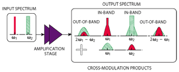
Figure 1 Dual-band transmission scenario.
Wireless communication systems are continuously growing to support more users with higher data rates while using a limited and already saturated radio frequency (RF) spectrum. To take advantage of the spectrum, spectrally efficient modulation schemes based on code division multiple access (CDMA) and orthogonal frequency division multiplexing (OFDM) are commonly used. These schemes have a non-constant envelope signal with a high peak-to-average power ratio (PAPR). This increases transmitter nonlinearities, while the requirements on the RF front end linearity performance are becoming tougher. The power amplifier (PA) plays a key role in the tradeoff between linearity and power efficiency.2
System Description
In a concurrent multi-band scenario (see Figure 1), the carriers are placed far apart from each other (typically greater than 100 MHz) driving a single amplification stage. Two types of distortion may be observed:
- In-band – Intermodulation products by a carrier in a band and also distortions introduced from other bands which fall in the intended transmission band.
- Out-of-band– All the intermodulation products that fall out of the transmission band that can be reduced using transmit or receive filters.
Due to ADC/DAC limitations, separate transmit and receive paths are necessary for each band, with independent local oscillators (LO). Each has the same bandwidth and sample rate requirement as a single band. A simple dual-band DPD block diagram is shown in Figure 2. It consists of two subsystems: an adaptation stage and a predistorter, or forward path.
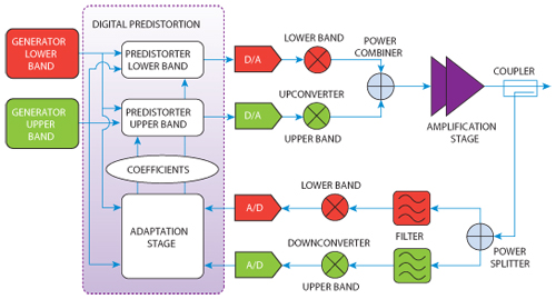
Figure 2 Dual-band DPD and power amplifier block diagram.
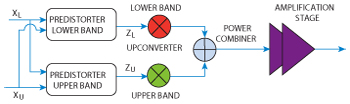
Figure 3 Concurrent dual-band predistorter block diagram.
The adaptation stage continuously estimates PA characteristics by utilizing samples from the transmitted data (before the DACs) and the observation path (after the ADCs). It employs a PA behavioral model that is described by the Volterra nonlinear model or one of its derivatives.2 The output is a set of filter coefficients that are passed to the predistorter. The coefficients can be stored in look-up tables for reuse. There are other components such as equalizers, alignment and power control blocks around the adaptation stage that process the samples for estimation.
The predistorter is a set of filters that apply coefficients, generated as a result of estimation, to the transmit data. Predistorter filters run with a sample rate that is at least 3 to 5 times greater than the signal bandwidth to compensate for third and fifth order intermodulation products. In order to maximize the predistortion bandwidth for a given FPGA frequency, polyphase designs can be used.3
Theory
This article focuses on the design of a concurrent dual-band DPD predistorter, also referred to as a frequency selective DPD.4,5 As mentioned previously, the predistorter must not only reduce in-band distortion (single-band scenario), but must also suppress cross-modulation products that fall into the transmission band. Out-of-band products can be rejected using transmit filters. The structure of the 2D-DPD predistorter is shown in Figure 3.
The Volterra series is a general nonlinear model with memory, but is not useful for practical applications due to its complexity and the large number of coefficients that must be estimated. Instead, the well-used single band memory polynomial model has been extended to the concurrent dual-band scenario by Roblin4 and Bassam.5 Both baseband DPD output signals ZL and, ZU, respectively,for the lower side band (LSB) and the upper side band (USB) can be expressed as follows:
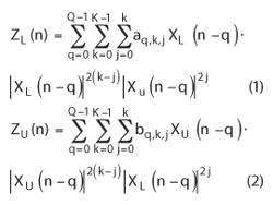
whereXL and XU represent both input band signals, and aq,k,j and bq,k,j represent the set of complex coefficients for the LSB and USB respectively. K represents the nonlinearity order and Q is the memory depth. From the PA output signals, the least-square algorithm8 is used to estimate the set of coefficients.
DPD Algorithm Development
The DPD method must meet standard requirements, be resource efficient on target platforms, must support rapid development and be flexible to change. It must also have the following properties:
- Enable the transmission and reception of many different waveforms including standard test patterns and custom carrier aggregation modes.
- Enable the testing of DPD in isolation from other radio head systems such as crest factor reduction.
- Facilitate performance bench marking for various algorithms and enable swapping components of a DPD solution.
- Provide design and hardware modularity.
The following development steps optimize the coexistence of simulation software and flexible hardware in an integrated platform. This ensures that the resulting DPD algorithm can be easily tailored for a specific set of standards, hardware implementation and PAs.
Step 1: Algorithm Simulations
Develop a DPD simulation model using a programming or scripting language such as Matlab. The purpose is to use flexibility and simplicity of software simulation environments to ensure DPD and related algorithms deliver the expected results and performance.
Step 2: High Level Synthesis Tools
After the algorithm is verified by simulation, decide which parts of the design are to be implemented in hardware. The most common approach is to realize the DPD predistorter filter in hardware on an FPGA and a use processor to run the adaption stage. To ensure that hardware components provide performance similar to software simulations, construct a hardware accurate model using a high level synthesis tool. The tools are often capable of generating RTL for target devices.
Step 3: System Level Integration
Once the hardware model demonstrates acceptable performance compared to software simulation results from Step 1, integrate the RTL into the communication system using standard interfaces and commercial integration tools.
Step 4: System In the Loop (SIL) Verification
Test and verify performance in hardware running jointly with simulation. In SIL verification, a functional block may exist only in software simulation or in hardware, or in both. As the blocks are modified or developed, they can be pushed into hardware and run in conjunction with software simulation for performance measurement and verification.
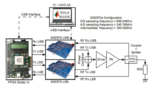
Figure 4 Dual-band DPD development platform.
Design Example: 2D-DPD Predistorter
MATLAB is used for software simulations and it accommodates algorithms and data processing scripts. It also contains Altera’s SIL APIs which enable communication with FPGA boards. For example, data can be written to DDR3 memory or a register value can be read back. A hardware accurate model of a DPD signal processing component is built in Simulink using Altera’s DSP Builder Advanced (DSPBA) block sets.6 DSPBA provides blocks of IPs for fixed and floating point operations7 and enables verification of components before hardware implementation. MATLAB and DSPBA can communicate and pass parameter values using workspace variables. RTL code is automatically generated from the DSPBA model to run on an FPGA.
The hardware platform consists of a number of Altera and third-party components as shown in Figure 4. On the digital side, a Stratix IV FPGA development board is used, which consists of DDR3 memory banks and standard USB and HSMC connectors. An analog front end with two LOs is required to support two widely separated bands. For this purpose Analog Devices MSDPD G 1.6 boards8 are used, where each has an independently programmable LO. Each board has a separate transmit path where the outputs are combined and fed into the PA. On the observation path, the PA output is split between the boards. It is important to ensure the distorting PA is biased correctly and sufficient attenuation is placed at the PA’s output for device protection. It should be noted that to saturate a PA, extra power can be provided with a chain of power amplifiers.
Performance
The 2D-DPD predistorters are simulated in MATLAB, verified in DSPBA and then implemented in an FPGA. The system consists of random access memory (RAM), direct memory access (DMA) and the predistorters. Transmit data is loaded from MATLAB to RAM, then played out through the predistorter on the FPGA using DMA. The PA output signal is also captured by RAM using DMA and then is read back to MATLAB. The adaptation stage continuously runs in MATLAB utilizing transmit and captured back data from the PA output. Communication between MATLAB and the FPGA is facilitated by SIL application program interfaces.
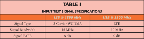
On the test bench, the LSB and USB center frequencies are set to 1890 and 2200 MHz, respectively. The amplification stage is composed of a linear driver followed by a broadband 10 W peak output power PA, based on the NXP Semiconductor GaN HEMT CLF1G0060-10 transistor. The signal characteristics are described in Table 1.
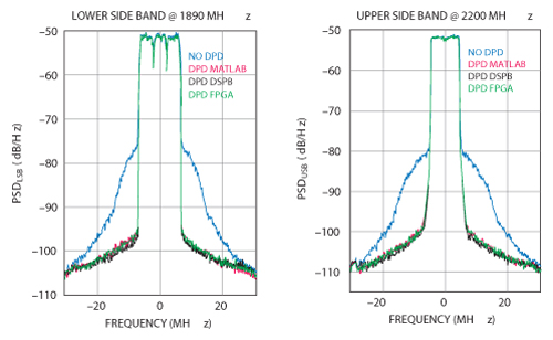
Figure 5 LSB and USB output spectra.
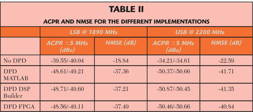
Digitaldown-conversion(DDC), time alignment and coefficients estimation are processed via MATLAB from the recorded PA output data. The training and the validation streams are composed of 8k and 131k samples, respectively. The DPD is implemented using 32-bit fixed point accuracy with a maximum nonlinearity set to K=4 and a maximum memory depth to Q=3. Figure 5 shows both LSB and USB output spectra of the PA with and without DPD for the three methods of implementation. In both bands, spectral re-growth is reduced as predicted by the three methods, which exhibit similar results. Table 2 compares DPD performance in terms of adjacent channel power ratio (ACPR) and normalized mean square error (NMSE) for both bands.
Conclusion
Practical challenges for dual-band DPD algorithm development are introduced and four development steps are outlined. The steps are performed using a development platform based on the Altera FPGA and other tools. Using this platform, a 2D-DPD predistorter is implemented on an FPGA. Its performance corresponds closely with MATLAB and Simulink simulations.
Acknowledgment
The authors would like to thank Analog Devices and NXP for their donations and technical support.
References
- F.M. Ghannouchi and O. Hammi, “Behavioral Modeling and Predistortion,” IEEE Microwave Magazine, Vol. 10, No. 7, December 2009, pp. 52-64.
- J. Vuolevi and T. Rahkonen, Distortion in RF Power Amplifiers, Artech House, Norwood, MA, 2003.
- “Designing Polyphase DPD Solutions with 28-nm FPGAs,” Altera Corporation, January 2012, www.altera.com/literature/wp/wp-01171-polyphase-dpd.pdf.
- P. Roblin, S.K. Myoung, D. Chaillot, Y.G. Kim, A. Fathimulla, J. Strahler and S. Bibyk, “Frequency-Selective Predistortion Linearization of RF Power Amplifiers,” IEEE Transactions on Microwave Theory and Techniques, Vol. 56, No. 1, January 2008, pp. 65-76.
- S.A. Bassam, M. Helaoui and F.M. Ghannouchi, “2-D Digital Predistortion (2-D-DPD) Architecture for Concurrent Dual-Band Transmitters,” IEEE Transactions on Microwave Theory and Techniques, Vol. 59, No. 10, pp. 2547-2553.
- www.altera.com/technology/dsp/advanced-blockset/dsp-advanced-blockset.html.
- www.altera.com/technology/dsp/floating-point/dsp-floating-point.html.
- www.analog.com/en/content/eb__Mixed_Signal_Digital_Pre-Distortion_sys_board/fca.html.