
The art and science of radio hardware design has been to some degree about minimizing, avoiding and, if possible, altogether eliminating unwanted spurious signals that find their way into the receive path of a radio. Typical sources of such signals are usually the multitude of two or more terminal devices that contain active semiconductor junctions such as diodes, transistors and ICs made up of them. These junctions with their nonlinear current voltage characteristics can be a rich source of harmonics and various intermodulation products, especially if more than one signal is present across them. Though magnetic materials commonly encountered in electronic circuits of most kinds are also a potential source of such nonlinearities, these components are usually used in blocking low level, low frequency ripples and occasional spikes in voltage or current and rarely interfere with communication signals unless poorly designed and selected.
One exception is the RF ferrites in the form of isolators and circulators. Such components, usually preceded by amplifiers, will generate and contribute to the harmonic and intermodulation content present in the outputs of such circuits. In a typical telecommunication system, such unwanted spurious signals will be eliminated and blocked before they have a chance to leak back into the receiver. Voluminous standards exist to ensure that such interferers are always well controlled and contained. Most RF engineers are usually well aware of these issues. These effects can be modeled and the theory behind them is well understood, so such nonlinear signal products can be analyzed and managed relatively easily.
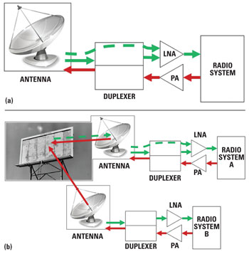
Figure 1 Shared apertures with multiple carriers can cause PIM to appear in the receiver of a duplex system (a) and external PIM generated beyond the antenna, either in combination with another transmitter or by reflection of the mixed transmit signal of the same transmitter by a nearby PIM generating object/obstacle (b).
There is another type of signal distortion that has become a great concern in wireless applications recently and that is passive intermodulation (PIM). This is the kind of intermodulation that is generated by passive components and interfaces. It is counterintuitive for most engineers and designers that totally passive components can produce intermodulation products, but they do and can degrade operation of advanced wireless services and even block radio links altogether if not controlled and managed properly.
What Causes PIM?
It is important to understand that typically there is no single and unique source of PIM and this is a general term for a whole category of intermodulation phenomena caused by passive elements in the path of an RF signal. It is also true that at the microscopic level, the actual process of PIM generation is still poorly understood. We know, for example, that poor contacts are the most common source of PIM. Poor contact may mean connectors not torqued to proper limits or poor quality of mating surfaces which may be the result of poor surface finish as well as presence of any contaminants such as flux, oxidation or loose particles. These result in mildly nonlinear contacts as opposed to clean ohmic ones. Dissimilar metals in contact may create diode-like effects also. Ferromagnetic material or coatings as well as certain types of PCB designs, metallization schemes and certain dielectric materials and coatings can generate PIM too.
Electro-thermal effects can cause PIM as well. Electro-thermal conductivity modulation in resonant structures like filters and antennas is very different in nature than other types of PIM since there are no dissimilar metals or even junctions or contacts involved.
When the antennas are also part of the consideration, then “external” PIM that is produced and introduced beyond the transmit antenna when single or multiple antennas reflect strong signals from nearby metallic structures is also a possibility. This is true for both indoor and outdoor installations.
As can be surmised from above, there are a wide variety of causes for PIM, from basic component design to quality of assembly and installation, and all will exist and contribute to total PIM at some level. It is important to realize that it may be unnecessary or even impossible to eliminate PIM altogether but it is critical that it stays below a certain level at locations where it may impact the receiver sensitivity.
What is the Problem?
The detrimental nature of PIM to radio reception has been well known for a long time by radar and satellite earth station engineers due to the shared antenna apertures for very strong transmit and very weak receive signals (see Figure 1). This also explains why PIM is typically a concern for infrastructure equipment and not for the user equipment.
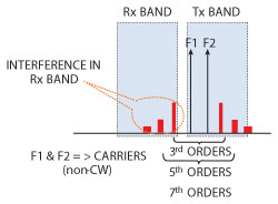
Figure 2 Odd-order IM products fall near the carriers themselves, sometimes within the Rx band of the same or another operator and cannot be filtered (note that IM bandwidth is n times the bandwidth of the fundamental tones for non-CW signals).
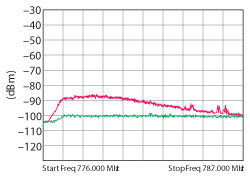
Figure 3 Rise in the noise floor of an LTE receiver due to PIM when the transmitter is turned on.
At the point or points of PIM generation along a transmit chain, the generated intermodulation products and energy will travel in both forward and reverse directions. If there is a path back to the receiver and if PIM has components in the passband of the receive chain (see Figure 2), then some of this energy will be mixed in with the actual receive signal as excess noise, as shown in Figure 3. In essence, PIM is always present in any RF system but the degree of it and where it ends up is the concern for good radio operation.
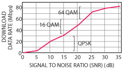
Figure 4 Downlink data rate in modern wireless systems is dependent on the signal to noise ratio at the receiver.
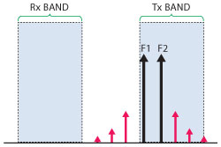
Figure 5 Many times the IM products generated will not fall into the Rx band, or those that do will have very high orders and negligible power.
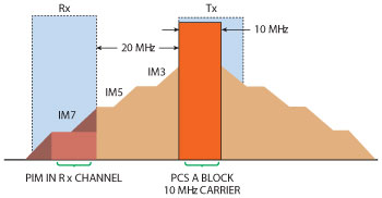
Figure 6 When broadband signals are involved, it does not take two carriers to generate PIM. A single broadband carrier will generate its own PIM also.
Use of an increasing variety of wireless bands and the need to share antennas to minimize non-recurring as well as recurring cost of wireless antenna installations, not to mention esthetic concerns, have exasperated PIM-related problems in recent years. In addition to shared antenna and other infrastructures, proliferating in-building wireless (IBW) systems, mainly distributed antenna systems (DAS), which also combine and consolidate high power macro base stations, small cells or repeaters create more opportunities for PIM problems. Also contributing to the problem are the higher data rates and the complex modulation schemes that enable them. High data rates are achieved only under good SNR conditions, where either the desired signal is strong with respect to all other noise and interference, or such noise is very small (see Figure 4). So while coverage is critical, good signal quality is just as critical now.
Consequently, any PIM in the receive band that will raise the noise floor, especially in a 4G receiver, and will be detrimental to receiver operation and achievable data rates. Note that not all PIM, even high levels, presents a problem for the receiver if it is blocked or out of the band of operation, as shown in Figure 5. It is also possible for a single broadband carrier to generate its own PIM due to self-mixing without a second carrier present (see Figure 6).
PIM Characteristics
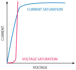
Figure 7 Unlike an amplifier where the source of nonlinearity is the current saturation, most of the nonlinearities that generate PIM are caused by voltage saturation due to imperfect contacts.
The very presence of PIM points to a nonlinearity in the signal path, of course. Thus we have to reach in our tool box of nonlinear analysis to understand, quantify and, most importantly, specify acceptable PIM levels in a system and for individual components used. Similarities to other types of nonlinearities, that we are all so familiar with in the RF world, can be misleading if relied on beyond the basics. Where the nonlinear theory is very precise and helpful is identifying where to expect the PIM signals to appear given the presence of the interacting high power signals/carriers. Regardless of the type and source of nonlinearity present, there will be odd- and even-order intermodulation products when anything other than a single CW tone is forced into the system. Thus we can precisely determine where the PIM will appear given a knowledge of the carrier frequencies. In a typical telecommunication application, it would be the third and other odd-order products that would be of interest.
The problem is our trusted nonlinear analysis and methods would be of little use in predicting typical PIM amplitudes. The sources of nonlinearities that cause PIM are not the semiconductor junction types we are more familiar with as previously discussed. Sources of nonlinearity may be a poor interface and ohmic contact. Current flow through such surfaces may involve tunneling type conduction. This is a very mild type of nonlinearity, closer to ohmic than a usual semiconductor junction (see Figure 7). There may be millions of such contacts in parallel with true ohmic contact points present in two contacting surfaces, thus creating a collective nonlinearity that is highly dependent on pressure, temperature, signal amplitude itself and maybe even time. It would be hard to expect such a system to follow a single power law. Note that the mechanism is not one of saturation either. To make matters worse, while some PIM sources are point sources, well localized, some are distributed. Various orders also add and cancel as a function of frequency and tone/carrier separation. Consequently, one cannot and should not make extrapolations that are typically made with better behaved nonlinearities, such as quantifying the nonlinearity and PIM by an IP3 of the system. Due to combined effects described above, it is not very unusual to observe 5th or 7th order PIM to have a higher observed power level than 3rd for example.
Data clearly indicates that PIM rarely follows the typical odd-order power law. For each dB increase in incident RF (tone) power, one rarely observes a 3 dB increase, or a 3:1 slope for IMD3, which nominally would be the strongest component (see Figure 8). More commonly, the observed slope lies somewhere between 1.5:1 to 2.7:1. It is also likely to be very frequency dependent. So, IP3 turns out to be a rather meaningless parameter in quantifying and specifying PIM. Similarly, one should not expect PIM to decrease by 30 dB (IMD3 component) because the RF excitation is 10 dB lower and vice versa. It rarely works that way in practice. The same applies to higher orders too, as seen in Figure 8b.
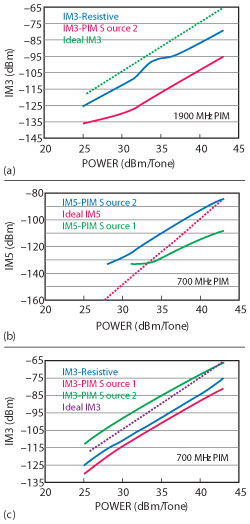
Figure 8 IM3 vs. power for two different devices compared with ideal at 1900 MHz (a), IM5s do not follow 5:1 slope either (b) and typical PIM IM3 rises 1.5-2.5:1 (c) (most set- ups are limited to near –140 dBm measurement by noise floor).
Avoiding PIM
The best method of assuring good PIM performance is to obviously start with guaranteed low-PIM components in the first place. Second, try to specify PIM as close to working conditions and power as possible to avoid needlessly expensive solutions. Given the infinite variety of conditions these components, subsystems and systems are used in, it is difficult to make up an all-encompassing standard. The closest we have to a standard is the IEC 62037-1 and -4 that specify the conditions for testing PIM and specifically in cables and connectors. These documents “recommend” the use of 2 × 20 W CW tones leaving the choice of frequencies and separation to the user per the needs of the system in use. These standards make no mention of the allowed maximum PIM level either. Again this is left to the discretion of the system designer or maintenance engineering since depending on the application and location, the requirements may vastly vary.
Meanwhile industry has developed ad hoc specifications for PIM, mostly based on field tests and trial and error. A maximum PIM level of –110 dBm in the receive band is usually what is desirable in many cases, especially when BTS interfaces are involved. Many component vendors aim for –118 dBm or better depending on the type of component. Given the standard test level of 43 dBm per tone (CW), this corresponds to a –153 dBc of PIM level. Note that it may be hard to relate this analytically to an ideal state-of-the-art receive sensitivity of around –120 dBm since these are defined for specific bandwidths and for CDMA/OFDM type signals that resemble anything but CW.
One of the drawbacks of a fixed power testing per IEC is its unsuitability to lower power applications. Designing and manufacturing a passive component or assembly for a 2 × 20 W test when, let’s say, the application is only 2 W, results in a costly and heavier solution than required. In the absence of a standard and accepted guideline, some users are inclined to stick with the 2 × 20 W test requirement which results in significant cost increase for the product. Even when the test requirement is pulled back to 2 × 2 W for example, the false expectation is for the PIM performance to be 30 dB better, around –140 dBm based on traditional IP3 analysis. This level is about –173 dBc from the test tone, the reliable measurement limit of many of the state of the art test instruments. It gets even worse if the PIM of specific interest is 5th or 7th order and one tries to apply textbook power laws. Then the requirement exceeds what is physically measurable. In Figure 8b, when reducing power down to 1 W per tone for example, the actual IM5 measured is about 25 dB higher than what a simple 5:1 extrapolation would predict. It is possible to lower PIM for a component to such low levels by careful design, numerous iterations and very well controlled manufacturing process, but it is unlikely to obtain a reasonable yield for commercial applications, in addition to being unnecessary for proper system operation. So there is an obvious need to rethink the PIM specifications as the base stations get smaller and power outputs get lower.
Some of the confusion can directly be traced to the convention of specifying PIM as a relative measure in dBc rather than an absolute. This has become a defacto standard method of PIM measure. In reality and practice, a radio receiver responds to power, not dBc. Sensitivity of the radio does not typically change with PIM or other low-level interference. Since in practice, power levels impinging on an aperture may vary from system to system or for different installations, one could, in theory, adjust the required dBc value based on 2 × 20 W measurement and establish the requirement appropriate for the actual power levels. This would be straightforward only if PIM behaved according to a known power law. It does not, as shown in Figure 8. So while higher power level components and systems are tested with a standard level of 20 W tones, which is likely to be a good figure of merit, lower power system specs still remain open to interpretation and requires better knowledge of specific operating conditions and receiver sensitivity requirements. Otherwise, trying to extrapolate from 2 × 20 W tests to lower power levels, without considering the actual absolute power levels involved and required, will result in unrealistic component and subsystem requirements which will drive the costs up and yields down.