
This article describes a method for designing a frequency-tunable antenna using a microelectromechanical system (MEMS) digital variable capacitor (DVC) as the tuning element in the antenna aperture. The design example targets a smartphone where the low frequency response of the antenna is tunable from 700 to 960 MHz while the high frequency response from 1710 to 2170 MHz remains fixed. Significant performance improvement is shown when compared to an impedance tuning approach.

Smartphone industrial design is trending toward larger screens, larger batteries, flatter designs, multiple cameras and metallic cases. In addition, wireless network operators are moving to LTE requiring 2×2 MIMO, as well as carrier aggregation (combined frequency bands) supported in LTE-Advanced. Carrier aggregation requires the RF front end to operate over multiple, widely-spaced frequency bands or over very wide frequency ranges. These trends are making space-constrained, cost-effective front ends more difficult to design. One approach is to use additional components with complex switching networks adding signal loss, cost and complexity. A better approach is to use tunable components including filters, power amplifiers and antennas.1
Considerable effort is being spent on improving the entire RF chain, including broadband, tunable power amps, tunable filters and tunable matching networks. While tunable matching networks can deliver more power to the antenna, a much more significant improvement is possible by improving the radiation efficiency of the antenna, particularly with antenna frequency tuning (AFT), which tunes the antenna in the aperture. Table 1 shows typical losses attributed to components in the RF front end. Reducing losses in the antenna can have a significant impact on overall efficiency.

Figure 1 Two types of antenna tuning.
Antenna radiation efficiency is affected by physical size of the antenna and the instantaneous bandwidth required. To cover a wide frequency band, it must be large or the efficiency will be low; yet the antenna’s physical size is constrained by industrial design trends. This makes the cellular antenna system a good candidate for tuning.
Antenna Tuning
Antennas are transition devices (transducers) between guided waves and free space waves. There are two forms of tuning in antennas: 1) Antenna frequency tuning (AFT), as mentioned earlier, and 2) Antenna impedance tuning (AIT) executed by adjusting the feed point match. Figure 1 illustrates the difference between AFT and AIT.
AFT optimizes the radiation efficiency of the antenna system, while AIT optimizes the power transfer between the transmission line feeding the antenna and the antenna terminals. AIT uses variable reactive components at the antenna feed point to adjust the power transfer. It is effective over narrow bands, but has limited impact when the frequency tuning range is several hundred megahertz because the antenna itself cannot be both high efficiency and broadband. AFT allows the resonance of the antenna structure to be changed, which optimizes the radiation efficiency over much wider bandwidths than AIT.
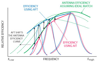
Figure 2 AFT compared to AIT.
Figure 2 shows the difference in efficiency between AFT and AIT. In this example, AFT shifts the total radiated efficiency curve for each tuning state, resulting in higher peak efficiency, whereas AIT follows a single antenna efficiency curve for each tuning state. Using AFT, the antenna can have 2 to 3 dB better efficiency than an antenna tuned using AIT, alone.
Design Method
The design method described in this article is for a multiband smartphone antenna and assumes that:
- Coverage is 700 to 960 MHz in the low band and 1710 to 2170 MHz in the high band.
- The low band is tuned while the high band is fixed.
- The antenna is a Planar Inverted F Antenna (PIFA), the most common for smartphones.
- The impedance match is fixed.
Key Device Characteristics
AFT is commonly used in military, civil and land mobile radio applications to tune narrowband antennas over wide frequency ranges. In these applications, the reactive elements are either variable capacitors or variable inductors and are typically large and expensive. For consumer electronic products, there are several device types that are candidates for tunable elements. They fall into two categories: variable capacitors and switches. Variable capacitance devices include varactor diodes, barium-strontium-titanate (BST) capacitors and MEMS devices. Switches include silicon on insulator (SOI), silicon on sapphire (SOS), gallium arsenide (GaAs) and MEMS devices. Switches can be used with discrete capacitors or inductors to create variable reactances or can be used to connect different antenna structures. A quick internet search will yield a large number of variable capacitors; however, due to the nature of these devices, there are no high performance, cost-effective, small, variable inductors on the market. This article focuses on using a variable shunt capacitor for antenna frequency tuning.

A device used for a frequency-tuned antenna in a smartphone must have the characteristics shown in Table 2. The two key characteristics that drive antenna efficiency are ESR and Cmin.
The Effect of ESR
The most important characteristic is low ESR. An ideal antenna with 100 percent efficiency will radiate all the power available at its input terminals without any losses. In practice, however, antennas have several loss mechanisms. Non-tunable antennas have losses due to impedance mismatch, conduction losses and dielectric losses. Tunable antennas have additional loss from the tuning devices. The goal is to minimize all of these losses. It is essential for the tuning capacitor to have the highest possible Q and the lowest possible ESR. The lowest losses require both low ESR and low capacitance. As shown in Figure 3, an ideal device (ESR = 0 Ω) adds no additional loss. Only one ohm can produce 2 to 3 dB of additional losses making ESR a critical parameter. Figure 3 also shows that lower capacitance loading further limits losses.
The Effect of Cmin
In addition to low ESR, the device must have low minimum capacitance (Cmin). Loading the antenna aperture with capacitance lowers the resonant frequency, making it appear electrically longer. To compensate, the antenna must be physically shortened. This shortening reduces radiation efficiency. Using the smallest amount of capacitance to load the aperture will result in the largest physical resonant structure and highest radiation efficiency. Figure 4 illustrates the importance of low Cmin and its effect on radiation efficiency. Lower Cmin improves radiation efficiency significantly in the lower band.
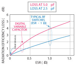
Figure 3 Losses due to ESR and capacitance.
The Effect of C Range
Tuning range is generally considered to be a key characteristic of a variable capacitor. For antenna frequency tuning, however, the capacitor tuning range is not so important. Figure 5 shows how an antenna can be designed to have the same frequency tuning range with a variety of capacitor tuning ranges. This is because the desired frequency tuning range is a design parameter that can be adjusted by selecting the capacitor location on the antenna aperture.
Feed, Ground and Digital Variable Capacitor Location
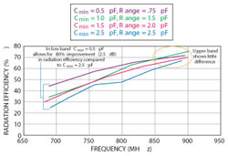
Figure 4 Impact of Cmin on radiation efficiency.

Figure 5 Required C range for a 200 MHz tuning range at various tuning locations.
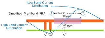
Figure 6 PIFA structure. Location 2 provides a wider tuning range than 1.
Figure 6 shows a sketch of a simplified multiband PIFA structure. Several parameters must be simultaneously optimized to produce a good frequency-tuned antenna design. The first is the location of the antenna feed point. Feed and ground locations are usually determined very early in the design phase and are dictated by industrial design constraints and available printed circuit board (PCB) real estate. The feed geometry is generally determined long before the antenna is designed, sometimes resulting in compromised performance. The best process to mitigate the risk of picking the wrong feed geometry is to make the layout as generic as possible.
Figure 7 shows a general schematic diagram allowing the feed and ground points of the antenna to be swapped during the antenna design phase. This layout gives the designer the choice of a normal or reverse-fed PIFA.
Variable Capacitor Connection to Antenna
The location of the tuning element is important and is also generally determined before the antenna design is complete. There are three basic methods to connect the tuning element to antenna (see Figure 8). Method C is the preferred method for connecting the capacitor because it is generally close to the antenna feed and ground due to industrial design and PCB layout constraints. This usually results in a suboptimum location, for which the antenna design can usually compensate.
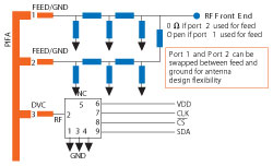
Figure 7 PIFA schematic allowing feed and ground to be swapped.
Variable Capacitor Tap Point
The variable capacitor location affects how much the frequency tunes with capacitance variation. The tap point can be modified by changing the location and length of the line that runs from the variable capacitor interconnect point to the PIFA low-band arm. Figure 9 illustrates the change in tuning slope relative to variable capacitor location. The farther out the capacitor is on the radiating element, the faster the frequency will change with capacitance.
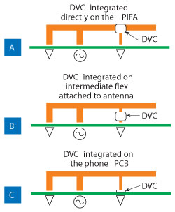
Figure 8 Methods for connecting the digital variable capacitor to the antenna.
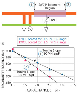
Figure 9 Change in tuning slope relative to DVC placement.
Variable capacitor location also affects how the high band (1710 to 2170 MHz) reacts with changing capacitance. It is possible to find a location on the antenna where tuning the low band will have no effect on the high band. Radiation efficiency, low-band tuning range and high-band performance are iterated to find the best antenna performance.
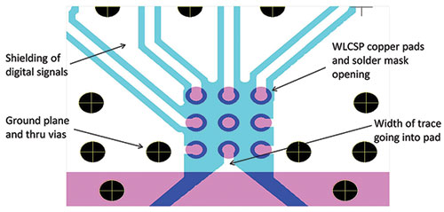
Figure 10 PCB layout that minimizes parasitics.
Impedance Matching Network Design
After determining an optimum device location, a fixed matching network is added at the feed point to optimize power transfer between the transmission line and the terminals of the antenna. The matching network is designed by measuring the complex impedance at several frequency points in the bands of interest using a vector network analyzer. The most effective frequency points to choose for optimization are the band edges and at least one point in the middle of each band to ensure that the matching network does not introduce unwanted narrowband behavior. The measured impedance values are entered into impedance-matching optimization software to obtain the best three-, four- or five-element match across the frequency bands of interest.
PCB Layout Considerations
Since antenna performance is dependent on reactive loading, it is important to minimize parasitic capacitance and inductance between the device and the antenna. This can be done by following good RF PCB layout practices. Figure 10 shows an example of proper PCB layout around a variable capacitor.
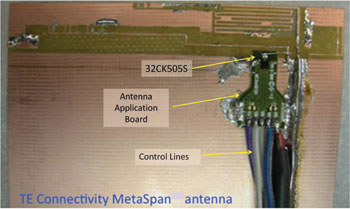
Figure 11 Frequency tuned antenna using a DVC driven by an applications board.
Mutual Coupling
Another parameter that must be considered is coupling between multiple antennas. MIMO operation in 4G systems requires at least two antennas. The interaction between antennas operating in close proximity to one another is called mutual coupling. In a MIMO system, the mutual coupling can be large because both antennas are operating at the same frequency at the same time. Energy coupled from one antenna to another cannot be recovered and lowers the efficiency of both antennas. In a MIMO system it is important to have high isolation between antennas.
Frequency tuning both the primary and secondary antennas in a MIMO system allows both antennas to be tuned and/or detuned to improve the isolation, lowering the mutual coupling and improving the efficiency. Tuning the main and diversity antenna separately can provide a large benefit in data rate throughput since the diversity gain is proportional to antenna isolation.
Measured Results
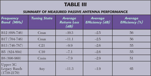
The key performance parameters for passive antenna evaluation are return loss and average gain (efficiency). Passive antenna parameters are shown in Table 3 for a multiband tuned antenna structure. For carrier qualification, the relevant active performance parameters are total radiated power (TRP) and total isotropic sensitivity (TIS). These measurements are taken on the completed phone assembly and are usually done in a controlled environment, such as an anechoic chamber. The phone is placed in the chamber and a call is initiated with a base station simulator (call box). Data is taken over a complete sphere to evaluate phone performance in all directions. The measurements are performed using phantom heads and hands to simulate the loading effects of the human body. At this stage of qualification, it is often necessary to tweak the antenna to optimize performance. This is where tunable antennas provide a big advantage. During active testing, tuning of both the primary and secondary antennas can be adjusted to optimize TRP and TIS. The tuning can also be adjusted to compensate for variations in the device usage model, mitigating head and hand detuning effects. The antenna tuning settings for various usage models can be stored in look-up tables and recalled during normal phone operation.
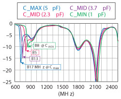
Figure 12 Return loss of TE Connectivity MetaSpan Antenna.
Passive Testing
Figure 11 shows a frequency-tuned antenna structure developed by TE Connectivity using the Cavendish Kinetics digital variable capacitor model 32CK505S. The antenna is on the edge of a 100 × 60 mm ground plane. Antenna dimensions are 60 × 10 mm. The 32CK505S is mounted on an antenna applications board which is soldered to the main board ground plane.
Figure 12 shows the return loss for the antenna and Figure 13 shows the measured efficiency. Table 3 summarizes the measured return loss and radiation efficiency for different frequency bands and capacitor settings. The data shows the low band of the antenna tuning from Cmin – Band 8 with a high-band edge frequency of 960 MHz down to Cmax – Band 17 with a low-band edge frequency of 704 MHz. As the low band is tuned, the high band from 1710 to 2170 MHz remains unchanged, demonstrating that a frequency-tuned antenna can have a tunable low band while keeping the high band fixed.
Active Testing
Industrial design features, such as the size of the display and battery, the thickness of the phone and the location of cameras and connector ports have a significant effect on antenna performance. The measured data shown in Figure 14 is a summary of the TRP from a complete smartphone assembly comparing AIT and AFT. The baseline performance identified as 100 percent on the chart is the performance of AIT in Band 17 and Band 5. The AFT performance is better in both Band 17 and Band 5. The performance in Band 17 (lower frequency band) is better than Band 5 due to the optimization of the fundamental antenna resonance in Band 5. This is similar to the performance shown in Figure 2.
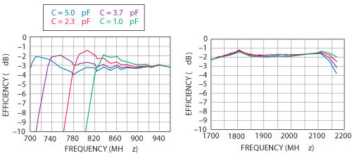
Figure 13 Measured efficiency of TE Connectivity MetaSpan Antenna.
Conclusion
Operator qualification requirements, industrial design constraints and consumer demand for high-speed data are driving the need for tunable RF front ends in smartphones. Antenna radiation performance is strongly dependent on smartphone industrial design constraints and is limited by the physical volume for antenna implementation making the antenna a good candidate for tuning. AFT (where the tuning element is part of the antenna aperture and is used to optimize radiation efficiency) is an effective form of antenna tuning; however, to tune the antenna and achieve a measureable benefit, the tuning element must have very low ESR (high Q), low Cmin and good tuning range.
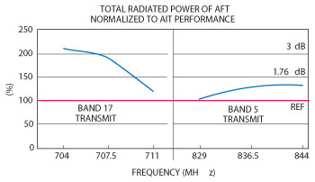
Figure 14 Active measured data comparison between AFT and AIT in a smartphone platform.
Several key design variables must be considered to design a good tunable antenna including feed, ground and tuning element location, tuning element connection to the antenna, tuning element tap point on the antenna, impedance matching network design, PCB layout to minimize parasitics, and mutual coupling to diversity and MIMO antennas. Measured data from a smartphone equipped with a DVC-enabled tunable antenna shows significant performance margin.
Reference
1. P. Carson and S. Brown, “Less is More: The New Mobile RF Front-End,” Microwave Journal, Vol. 56, No. 6, June 2013.
Paul Tornatta has more than 25 years of experience in the aerospace, wireless, telecommunications and automotive industries. Before joining Cavendish, he served as CTO of Skycross, a leading mobile antenna supplier. Prior to that, he served as vice president of the automotive business unit at Radiall Corp., a leading supplier of RF interconnect products. He also served in a variety of leadership positions at Larsen Antenna Technologies, Metricom and Lockheed Martin. Tornatta earned a bachelor’s degree in electrical engineering from New Mexico State University. He has written articles on RF design and electromagnetics for a variety of RF trade publications. He is a member of IEEE.