
With the implementation of the European RoHS directive, lead-free mandates have resulted in obsolescence of commercially available electronic components with tin-lead finishes. This raises the risk of system failures as related to tin whisker formation as a tin finish without lead can ultimately develop conductive tin whiskers that result in electrical shorts within circuitry.
Mission critical applications requiring tin-lead finishes need to establish other design approaches or consider mitigating RoHS components that are only available with pure tin finishes. The first option is not practical given that alternate component options are not commercially available with tin-lead finishes. This article will explore a tin whisker mitigation process applicable to both passive and active components that utilizes a thermo-chemical fusion process in order to prevent whisker formation.
Background
Tin whiskers are single crystal filament growths that are known to achieve lengths of up to one inch. Tin whiskers grow unpredictably on pure tin surfaces and whiskers can cause catastrophic short circuits as they are conductive.
Pure tin, which contains less than 0.1 percent lead, is a high reliability risk because of its propensity to form tin whiskers. There is a consensus that at least 3 percent lead is needed to prevent tin whisker formation. To date there is no clear understanding of the mechanism of tin whisker growth although stresses, internally and externally, to the tin surface are believed to be contributing factors.
Globally, electronic components continue to move toward lead-free finishes and solder assembly with continued implementation of the European RoHS directive. Certain countries, such as the United States, have not mandated similar directives, but have no choice other than to follow suit given that their products are sold worldwide.
Issues with Lead-Free
Components need to withstand higher circuit board assembly temperatures. Lead-free solders typically require re-flow temperatures of 40°C and above that of tin-lead alloys. Instead of 220°C for tin-lead, lead-free solders are typically recommended to re-flow at 260°C. Aside from equipment conversion costs, components and circuit boards have to be manufactured to withstand typical lead-free soldering temperatures of 40°C higher than tin-lead.
Two separate but related issues stand out with lead-free:
- Lead-free solders
- Lead-free plating
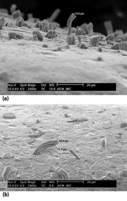
Figure 1 Tin whiskers on a multilayer ceramic capacitor - precious metal construction (a) and base metal construction (b).
Wetting properties of no-lead solders are not as good as tin-lead.1 Actually, the same reference also cited tin-lead as more stable than other tin based no-lead alloys as measured by their electrode reduction potential. Wetting difficulties could lead to voids in the solder joint.
Leaded components can be solder dipped, but chip size components (01005 and larger) must use plating techniques to yield solderable surfaces. For inexpensive passive chip components, palladium-nickel, the only other commonly used plating for components besides tin-lead and pure-tin, would raise the price beyond being competitive. What is left is only pure-tin if lead were to be eliminated.
The most critical lead-free issue has to be the propensity of pure-tin plated components to develop whiskers. As of yet there is no pure-tin plating that can claim to be whisker-free even those claiming to offer stress relief through a “matte” finish. Whiskers appear at unpredictable times and neither the onset conditions nor the growth habits are well understood. Furthermore, there is no accepted tin whisker growth acceleration method. From the body of knowledge on this subject, pure-tin plating will form whiskers under certain sets of unpredictable conditions.
Tin Whiskers
For tin whisker formation, a current theory is that diffusion related to intermetallic formation may cause stresses in the tin layer that are relieved with whisker growth; additionally, stresses related to the component’s environment (i.e. thermal, mechanical, electrical, atmospheric) may contribute as well. Stresses can also come from the plating conditions, from the substrates, or from external scratches/bends on the pure-tin surface. Organic brightener additives that give shine but add stress to tin plating are theorized to contribute to whisker growth while a “matte” tin finish without the additives is less prone to grow whiskers.
It is further theorized that copper substrates are more prone to form whiskers than other metals because of the formation of tin-copper intermetallics where the volume increase contributes to stress on the tin-layer. Additionally, tin-nickel intermetallics are also well known and tin whiskers can grow with either precious metal ceramic chip capacitors (silver electrodes, silver termination and nickel barrier below the tin) or base metal (nickel electrodes, copper termination and nickel barrier below the tin) versions of the same OEM device. Both versions of this pure-tin ceramic chip capacitor grew measurable whiskers after 88 temperature cycles from -55° to +85°C. See Figure 1 which shows tin whisker formation.
Ways to Avoid Tin Whiskers
Until there is an accepted accelerated test for tin whiskers, pure-tin finishes will be prohibited in mission critical programs where failure is not an option. Prohibition of pure-tin usually takes one of two forms: blanket prohibition for a program and prohibition by program risk. The latter is an attempt to quantify the risk in terms of program life and difficulty of equipment replacement to justify the costs of enforcing blanket prohibition of pure tin. Risk assessment is weighing the necessity of whether the risk of tin whiskers is worth the efforts and expense of guarding against pure tin from “sneaking” into electronic components and assemblies.
Enforcement of pure-tin prohibition across an entire program could take one or more steps from the following sequence:
- Procurement/subcontract vendor notices
- Incoming materials inspection
- Mitigation of materials available only in tin plate
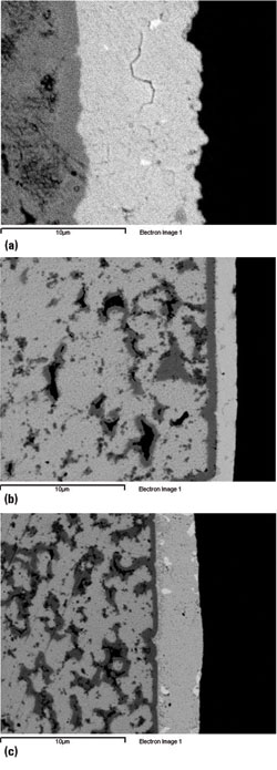
Figure 2 SEM photo of historic industry baseline solder plate, ~3% lead (a), pure-tin plate, (b) and fusion processed for tin whisker mitigation, 5%+ lead (c).
Pure-tin prohibition is usually enforced on the vendor side through notices first in quote or bid activities and later in requirements within purchase orders. Vendors and their distributors are then required to provide certification that the product shipped does not contain exposed pure-tin. This requirement is more easily met at the factory level than at the distributor level since there are clearer identifications of product and product coding at the factory level. Risks increase with increased product handling, especially with components that are not clearly marked with catalog number and lot date codes. With unmarked chip size components this could be a problem even at the factory level, especially since a single factory is likely to produce both versions. With the likelihood that components get re-reeled, the mix-up between pure-tin and tin-lead components at the distributor level is understandably tenuous.
Incoming materials inspection to guard against accidental receipt of pure-tin products is usually the next level of assurance. Incoming materials inspection is practiced in high reliability industries such as space and medical. The added tool to protect against pure-tin is the X-ray fluorescence (XRF) at the receiving dock. Handheld XRF machines are available and are calibrated to detect lead in components, enabling easier analysis on a lot sampling basis. Alternatively, samples from the incoming lot could be sent to analysis laboratories for Energy Dispersion, X-ray Spectroscopy (EDXS) using the same principle as XRF. Mostly, inspectors look for a minimum three percent lead content, the level commonly found in formerly ubiquitous tin-lead “solder plate.”
Blanket prohibition of pure-tin plate is currently practiced where the offered electronic equipment is to be “fail safe.” This includes industries in the satellite, space exploration, medical devices, missiles and other high-technology weapons or where life and limb are at risk. However, blanket prohibition is possible only when other acceptable plating or mitigation methods are still available (or where re-designs are possible to use alternative components that are still available in tin-lead).
Tin whisker mitigation of electronic components can be divided into two main categories, leaded and un-leaded surface mount technology (SMT) devices.
- Leaded active or passive devices: Pure-tin leaded devices can be dipped in standard tin-lead solder. Preheating can prevent thermal shock which can lead to cracking and de-lamination. Robotic handling improves precise dipping angle and travel. However, it is very difficult to dip inside the meniscus at the lead egress points of leaded devices, which increases the chance of potential tin whisker growth in these areas. Additionally, dipping of chip components introduces the risk of thermal shock and terminal coverage variation.
- SMT chip size active or passive devices: Pure-tin plated chip-size devices are too small and not practical to dip in tin-lead solder. To do so would risk the chance of thermal shock and present handling problems during dipping especially for small case sizes such as 01005 and 0201. The ideal mitigation would convert pure-tin into the previously universally used “solder plate” with at least three percent lead content.
Fusion Processing
The concept behind the fusion process is to treat the pure-tin plated terminal to give it solder plate attributes of five percent lead content. This is achieved by adding lead to the pure-tin plating. Furthermore, the lead must be evenly distributed in the entire pure-tin plated area which is accomplished through a low temperature fusion process that melts the tin and tin-lead and homogenizes the two layers into a monolithic tin-lead layer.
Figure 2 shows scanning electron microscope (SEM) cross-sectional pictures of a typical terminal of a ceramic electronic chip component. Under back-scatter scans in the SEM, lead particles are white and tin is the lightest gray and outer-most layer to the right. The dark gray area immediately adjacent to the left is the nickel barrier (see Figure 2a). This termination cross section is representative of the historic industry standard of approximately three percent lead, achieved by co-plating tin lead (typically 90-10) in methanesulfonic acid (MSA) solution. Again, this co-plating is known commonly as “solder plate.” Figure 2b shows the cross-section of a typical pure-tin version of the same device produced by the same manufacturer; the light gray tin area has no lead, and no visible white particles. Figure 2c is the same pure-tin micrograph 2b chip component after fusion re-processing. Notice the distribution of lead (white particles) throughout the previously pure-tin layer; with minimum of five percent lead there is additional security from a tin whisker mitigation standpoint.
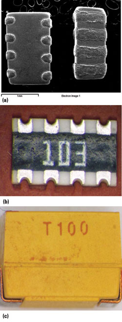
Figure 3 Components processed with fusion TWM process; chip capacitor array (a, b) and tantalum chip capacitor (c).
Capability of Fusion Processing for Tin Whisker Mitigation
Fusion processing for tin whisker mitigation (TWM) can be effective with the following:
-
All passive monolithic chip components where:
- Tin plating is part of the termination process
- Component is intended for solder assembly
-
Some passive SMT components where:
- Pre-tinned leads are molded
- Component is intended for solder assembly
- Some active discrete SMT chip size, components
TWM utilizing fusion processing may not be as effective where components have open sub-assemblies (i.e., wire-wound chip inductors, devices with radial leads, or tightly formed reverse J-leads). If there is any doubt, pre-evaluation testing is performed. For products where no source of tin-lead plated terminations are available, solder dipping appears to be the best short term solution for leaded components.
Figure 3 shows examples of passive components that have been processed using the fusion TWM process. The resistor and capacitor chip arrays were fusion processed with all 24 surfaces passing XRF and EDXS screening for five percent minimum lead content. The tantalum chip capacitor fusion process resulted in the inside and outside surfaces of the formed leads passing XRF and EDXS screening for five percent minimum lead content as well.
A current (but not limited) listing of compatible component types for the fusion TWM process is:
- Surface mount chip capacitors (01005 to 2220 package size or larger)
- Surface mount chip resistors (0402 to 2220 package size or larger)
- Surface mount chip inductors (0402 to 1812 package size or larger)
- Surface mount chip beads (0402 to 1812 package size or larger)
- Surface mount fuses (0402 to 1812 package size or larger)
- Surface mount varistors (0603 to 1812 package size or larger)
- Resistor arrays/capacitor arrays/chip bead arrays
- Molded body diodes (SMA, SMB, SMC, SMD packages with reverse J-leads and molded body MOSFETs)
- DPAK packages
- SOT-23 and SOT-223 packages
- DO-214AB package
- QFN packages
- Tantalum capacitors (all standard sizes)
- Lug connectors
- EMIFL packages and most chip and molded body filters.
Conclusion
Tin whisker growth is a high reliability risk when pure-tin is present anywhere in the electronics assembly. The fact is that when there is pure tin, whiskers may appear. The onset is unpredictable, but inevitable. As of right now there is no definitive theory of tin whisker genesis, nor is there an accepted accelerated whisker test method to validate these claims. There are a lot of activities in industry, government and academia to develop and qualify an accelerated whisker test methodology as well as understand tin whisker growth and prevention. CALCE and NASA (especially Goddard Space Center) are active in this endeavor, as is the industry group iNEMI.
References
1. Samsung Electronics, Evaluated Technical Data: “The Comparison of Reduction Potential on Materials.”
2. CALCE Tin Whisker Site, www.calce.umd.edu/tin-whiskers/
3. NASA Tin Whisker Site, http://nepp.nasa.gov/WHISKER/