
Opto-electronic components used in the high-speed data and telecommunications industries are susceptible to the effects of humidity, temperature variations and other physically and chemically demanding environmental conditions. With the growing trend for replacing electrical signals with optical ones, the importance of protecting these opto-electronic components is also growing.
A reliable, long-term protection of highly sensitive electronics is achieved by using hermetic housings. With world-leading competences in glass-to-metal sealing, ceramic-to-metal-sealing as well as full ceramic packages, Schott’s electronic packaging business unit offers all hermetic housing technologies from one source. This enables the optimization of the packaging in consideration of the many different performance criteria.
DESIGNING COMPACTNESS
Many RF packages, for instance, are Butterfly packages. The lead frame of these packages has the same height as the RF signal inside the package to achieve an RF path with low reflection. However, for connecting with the lines on the host board, such a package requires a cut out in the host board or bent leads. These options are far from ideal for technical, design and assembly reasons.
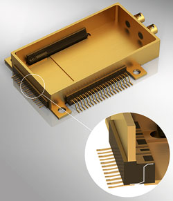
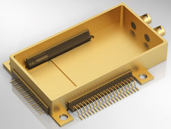
Figure 1 Surface-mount RF package with four differential line pairs, allowing for a data rate of up to 28 Gbit/s per pair.
For cost-efficient assembly, many customers prefer surface mount packages. Schott has recently developed a space-saving, standard-looking SMD package (see Figure 1) with a bandwidth greater than 30 GHz that allows for a highly customizable design of the package interior, while the outside package I/Os look pretty much standard. The height difference between the RF signal inside the package and the host board is bridged with a sophisticated hermetic multilayer ceramic package feedthrough.
MULTILAYER CERAMICS
The strength of multilayer ceramics lies in the high number of electrical feedthroughs that can be connected in a complex manner to achieve a dense routing inside a very small hermetic unit. High Temperature Cofired Multilayer Ceramics (HTCC) are mainly used for their high mechanical and temperature stability. They can easily be integrated into metal housings via high temperature brazing due to their matched thermal coefficients of expansion.
For special miniaturization and performance needs, Low Temperature Cofired Multilayer Ceramics (LTCC) offer a low dielectric constant and allow for the use of high conductivity metal as well as for embedding passive components such as resistors, inductors or capacitors. In general, multilayer ceramics are indispensable when it comes to miniaturizing opto-electronic components for use in the high-frequency range.
DESIGN CHALLENGES
The design and simulation of high performance fiber optical and telecommunication products is very important and Schott works closely with ix-cad GmbH, which provides computer aided design and simulation. For an opto-electronic package, several design challenges need to be solved: The height difference of the planar waveguide for the signal path inside the housing and the host board needs to be bridged. The signal propagation direction has to be turned from the horizontal direction into the vertical direction and once again into the horizontal direction to finally go through the ground plane in an inner layer (see Figure 1, cross-section).
To keep the impedance of the waveguide at this transition at the desired value, e.g., 50 Ω, the dielectric and metallic structures are designed in various geometries. Then, the electromagnetic (EM) field is simulated and the feedthrough is tested at ix-cad GmbH. The virtual prototyping process allows for quick modifications to achieve the optimal design. It significantly reduces development costs and shortens the time-to-market.
An additional benefit of this approach is that one can analyze the EM field inside the model and get insights into its behavior to improve the signal path quality. The simulation results show the insertion loss and the return loss and enable an optimization of the performance. The goal of this method is to achieve first-pass success with the prototype.
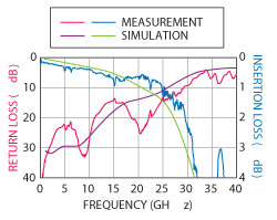
Figure 2 Simulated and measured return loss (S11) and insertion loss (S11) of the package feedthrough.
COMPLETE SIMULATION
All transitions of the feedthrough are modeled and optimized separately. Finally, the complete feedthrough is designed, including the transition to the host board. The next step is to produce the prototype and verify the performance. Figure 2 shows the measurement and simulation results of a high frequency package feedthrough including the connection to the host board in a frequency range from 1 to 40 GHz.
The height difference between the RF level inside the package and the host board may be several millimeters. In the example shown in Figure 2, the measured insertion loss (S21) displays a 3 dB bandwidth of 31 GHz. The measured return loss (S11) is < 10 dB up to 30 GHz. Simulation and measurement results fit well and demonstrate that this development process is based on the right model and enables enhanced and innovative designs of hermetic hybrid packages.
Schott Electronic Packaging,
Landshut, Germany
+49 (0)871/826-329,
ep.info@schott.com
www.schott.com/epackaging
ix-cad GmbH,
Eichenau/Munich, Germany,
www.ix-cad.com