
This article presents a new dual passband filter using hybrid microstrip split ring resonators and coplanar waveguide (CPW) quarter wavelength resonators. Its equivalent RLC circuit model is presented, in which the parameters are extracted from the theoretical analysis and the measured S-parameters. The proposed filter has two passbands with center frequencies of 2.44 and 3.5 GHz. Good agreement between the equivalent circuit (EC), the electromagnetic (EM) simulated and the measured results is demonstrated.
Filters with multiple passbands are an essential element for communication systems, which could achieve higher speed and higher capacity data transmission capabilities.1,2 In initial investigations, the dual passband filter has attracted much attention, and several design approaches have been proposed. Dual passband filters have been realized by parallel connection of two bandpass filters with different center frequencies.3,4 However, this configuration increases the size of the circuit. Another dual passband filter was obtained by using stepped impedance resonators (SIR) and quarter wavelength resonators,5 but it is difficult to achieve two adjacent passbands using SIRs. Besides, the short end of the microstrip quarter wavelength has to be realized via a drilled hole.
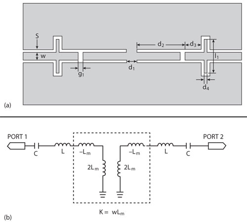
Figure 1 Structure of the bandpass filter with CPW quarter wavelength resonators (a) and its equivalent circuit (b).
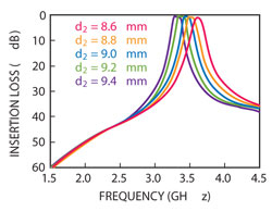
Figure 2 Bandpass characteristic as a function of d2.
In fact, coplanar waveguide (CPW) is a much more attractive approach for quarter wavelength short circuit stubs, due to its uniplanar structure. It has been getting more and more attention for its advantages, such as easy connections in series and shunt without via holes, insensitivity to substrate thickness and low dispersion effect in microwave and millimeter wave circuits’ design.6-8
Here, a dual passband filter is presented, using hybrid microstrip split ring resonators and coplanar waveguide quarter wavelength resonators. The microstrip split ring resonators and the CPW quarter wavelength resonators are symmetrically distributed on the top and bottom layers. A CPW input/output feed line is adopted in this structure. Finally, the filter is fabricated, with center frequencies of 2.44 and 3.5 GHz, which could be used for wireless local area network (WLAN) and WiMAX. The EM simulated and measured results are offered to demonstrate the characteristics of the proposed dual passband filter.
Filter Design
CPW Quarter Wavelength Resonators
The structure of the bandpass filter with CPW quarter wavelength resonators is shown in Figure 1. One end of the resonator is terminated by an open gap and the other end is terminated by a short circuited stub. The two neighboring resonators are inductively coupled and its coupling circuit can be expressed by K-inverters.9 The equivalent circuit of this structure is also shown in the figure. Its external quality factor is controlled by adjusting the width g1 of the coupling gap, while the coupling coefficient of the two neighboring resonators is adjusted by varying the width d1 of the coupling length.
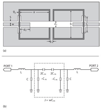
Figure 3 Structure of the bandpass filter with SIRs (a) and its equivalent circuit (b).
The bandpass characteristic of this filter is shown in Figure 2, with the dimensions: w = 1.6 mm, s = 0.5 mm, g1 = 0.2 mm, d1 = 1 mm, d3 = 5.1 mm, d4 = 0.5 mm, l1 = 6.7 mm and d2 is varied from 8.6 to 9.4 mm. The simulated results show that the center frequency of the filter is controlled by the resonant stub, which is approximately one quarter waveguide length.
Microstrip Split Ring Resonator with CPW Feeding Line
The structure of the bandpass filter with microstrip split ring resonators and CPW feeding line is illustrated in Figure 3. It is realized by a conventional microstrip split ring resonator on the top layer, with capacitive coupling to the CPW feeding line at the bottom layer. The input and output CPW feeding lines are connected by a slotline at the bottom of the split ring.
The two microstrip split rings are electrically coupled and the coupling circuit can be expressed by J-inverters.9 The equivalent circuit of this structure is also shown in the figure. The external quality factor is mainly decided by the coupling length l1 between the top split ring and the bottom CPW feeding structure. The coupling intensity is mainly affected by the separation distance t1.
The bandpass characteristic of this filter is shown in Figure 4 with the dimensions: w = 1.6 mm, s = 0.5 mm, g2 = 0.5 mm, d3 = 5.1 mm, l1 = 6.7 mm, e1 = 3 mm, t1 = 1.2 mm, a = 13.2 mm and b varied from 10.5 to 14.5 mm. It is found that the center frequency of the filter is influenced by the perimeter of the microstrip split ring resonator, which is approximately one half of the guided wavelength.
Dual Passband Filter Design
When the two bandpass filters analyzed here are connected together with CPW input and output feeding lines, a dual passband can be achieved. The layout of the proposed dual passband filter is shown in Figure 5. It is composed of a pair of coupled microstrip split ring resonators on the top layer and CPW quarter wavelength resonators at the bottom layer. A CPW feeding structure is introduced to feed this configuration.
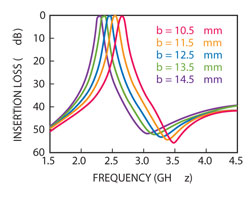
Figure 4 Bandpass characteristic as a function of b.
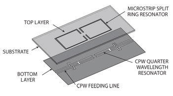
Figure 5 Layout of the proposed dual passband filter.
Following the general theory of couplings, the bandpass design parameters are calculated by:10
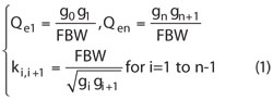
where Qe1 and Qen are the external quality factors of the resonators at the input and output, while ki,i+1 are the coupling coefficients between the neighboring resonators.
Using the commercial software Ansoft HFSS, based on the finite element method, the desired physical dimensions of the proposed dual bandpass filter could be determined. The external quality factor and the coupling coefficient are achieved by:11
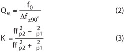
where f0 is the resonator frequency; Δf±90° is the absolute bandwidth between the ±90° point; and fp1 and fp2 are defined to be the lower and higher of the two resonator frequencies, respectively. After simulation, the final optimized parameters of the filter are as follows: w = 1.6 mm, s = 0.5 mm, g1 = 0.2 mm, g2 = 0.5 mm, d1 = 1 mm, d2 = 9.1 mm, d3 = 5.1 mm, d4 = 0.5 mm, l1 = 6.7 mm, a = 13.2 mm, b = 12.5 mm, t1 = 1.2 mm and e1 = 3 mm.
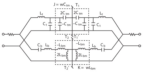
Figure 6 Equivalent circuit of the proposed dual passband filter.
Figure 6 illustrates the equivalent circuit of the proposed dual passband filter. The inductive coupling circuit and the capacitive coupling circuit are expressed as K- and J-inverter, respectively. The K-inverter is equivalent to a T inductance network, while the equivalent circuit of the J-inverter is a π capacitance network.
According to the theory of coupled resonator circuits, the inductive values of the equivalent circuit are described by:11
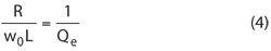
where w0 is the center frequency of the passband and R is the input impedance, which is set as 50 Ω.
Here the coupled-resonator circuits of the proposed filter are synchronously tuned. Then, in the odd model, the symmetry planes T1-T1' and T2-T2' are replaced by an electric wall, the resultant circuits have the respective resonant frequencies:
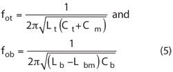
Equation 5 shows that the resonant frequency is lower than that of an uncoupled single resonator in the electrical coupling structure, while the resonant frequency is higher in the magnetic coupling. Similarly, in the even model, by replacing the symmetry planes T1-T1' and T2-T2' with a magnetic wall, the circuits have the respective resonant frequencies:
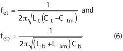
In this case, it turns out that the resonant frequency is increased in the electrical coupling, while in the magnetic coupling, the frequency is shifted down. From Equations 5 and 6, the mutual capacitance Ctm in the electric coupling circuit model and mutual inductive Lbm in the magnetic coupling circuit model are computed by:9
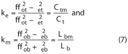
where ke is the coupling coefficient of the electric coupling model and km is the relevant parameter of the magnetic coupling model. Their values can be achieved by using Equation 1.
The center frequencies of each passband are calculated by:
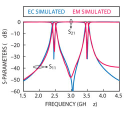
Figure 7 EM and EC simulation results of the proposed dual passband filter.
On the basis of the analysis illustrated, the values of the parameters in the equivalent network are obtained. First, by using Equation 1, the external quality factor and coupling coefficient of each passband are achieved. Then by substituting these values into Equations 4 and 8, the values of Lt, Ct, Lb and Cb are obtained. Finally, by inserting the obtained values into Equation 7, the mutual capacitance Ctm and mutual inductive Lbm are obtained.
Using the Advanced Design System (ADS) for the proposed dual passband filter, the values of the parameter in the equivalent network are: R = 50 Ω, Cb = 0.01755 pF, Lb = 118.52 nH, Lbm = 2.2249 nH, Lt = 106.02 nH, Ct = 0.03971 pF and Ctm = 0.001195 pF. The EM and EC simulated results of the proposed dual passband filter are shown in Figure 7. It depicts a dual passband filter with center frequencies of 2.44 and 3.5 GHz and the 3 dB fractional bandwidths are 4.17 and 2.86 percent, respectively. Good agreement between the analysis of the equivalent circuit model and the electromagnetic simulated proves the validity of the design method.
Experiment and Results
In order to validate the proposed dual passband filter, it was fabricated on a substrate with a relative dielectric of 9.6 and a thickness of 1 mm. The input/output impedance of the feeding lines is equal to 50 Ω, corresponding to the coplanar waveguide, which has a central strip width w = 1.6 mm and a slot width s = 0.5 mm. Figure 8 shows the photograph of the fabricated dual passband filter with dimensions of 40 × 50 mm.
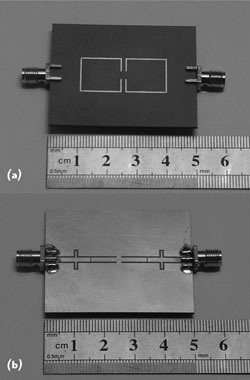
Figure 8 Photographs of the proposed dual passband filter. Top view (a) and bottom view (b).
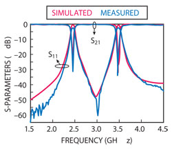
Figure 9 Measured and simulated frequency responses for the dual passband filter.
The experimental results were obtained from an Agilent vector network analyzer N5230A. The simulated and measured S-parameters are illustrated in Figure 9. The two passbands are centered at 2.44 and 3.5 GHz, which are used for WLAN and WiMAX. The return losses are better than 30 and 34 dB at the respective passband. The measured minimum insertion losses are approximately 1.91 and 1.74 dB in the lower and upper passbands, respectively. Comparison between simulated and measured results indicates a good agreement.
Conclusion
In this article, a dual passband filter using hybrid split ring resonators and CPW quarter wavelength resonators is modeled in theory and verified with experiment. An equivalent circuit is given to demonstrate the characteristics of the proposed filter. Its corresponding parameters are also extracted from the theoretical analysis. A dual passband filter covering center frequencies of 2.44 and 3.5 GHz was fabricated to validate the design process. The measured results have shown good agreement with the EM and EC simulated results. The proposed dual passband filter is useful in dual band wireless transmitting systems.
References
- M. Brandolini, P. Rossi and D. Manstretta et al., “Toward Multi-standard Mobile Terminals - Fully Integrated Receivers Requirements and Architectures,” IEEE Transactions on Microwave Theory and Techniques, Vol. 53, No. 3, March 2005, pp. 1026-1038.
- H. Miyake, S. Kitazawa and T. Ishizaki et al., “Miniaturized Monolithic Dual Band Filter Using Ceramic Lamination Technique for Dual Mode Portable Telephones,” 1997 IEEE MTT-S International Microwave Symposium Digest, pp. 789-792.
- C. Chu-Yu and H. Cheng-Ying, “A Simple and Effective Method for Microstrip Dual-band Filters Design,” IEEE Microwave and Wireless Components Letters, Vol. 16, No. 5, May 2006, pp. 246-248.
- F.C. Chen, Q.X. Chu and Z.H. Tu, “Design of Compact Dual- and Tri-band Bandpass Filters Using l/4 and l/2 Resonators,” Microwave and Optical Technology Letters, Vol. 51, No. 3, March 2009, pp. 638-641.
- A. Sanada, H. Takehara and T. Yamamoto et al., “l/4 Stepped-impedance Resonator Bandpass Filters Fabricated on Coplanar Waveguide,” IEEE MTT-S International Microwave Symposium Digest, pp. 385-388, 2002.
- H. Chen and Y.X. Zhang, “Dual-band Filter Using Composite Microstrip/CPW Structure,” Electronics Letters, Vol. 44, No. 16, July 2008, pp. 979-980.
- J. Shi, J.X. Chen and Q. Xue, “A Quasi-elliptic Function Dual-band Bandpass Filter Stacking Spiral-shaped CPW Defected Ground Structure and Back-side Coupled Striplines,” IEEE Microwave and Wireless Components Letters, Vol. 17, No. 6, June 2007, pp. 430-432.
- F. Martin, F. Falcone and J. Bonache et al., “Analysis of the Reflection Properties in Electromagnetic Bandgap Coplanar Waveguides Loaded with Reactive Elements,” Journal of Electromagnetic Waves and Applications, Vol. 17, No. 9, April 2003, pp. 1319-1322.
- J.S. Hong and M.J. Lancaster, Microstrip Filters for RF/Microwave Applications, John Wiley & Sons, New York, NY, 2001.
- J.S. Hong and M.J. Lancaster, “Couplings of Microstrip Square Open-loop Resonators for Cross-coupled Planar Microwave Filters,” IEEE Transactions on Microwave Theory and Techniques, Vol. 44, No. 11, November 1996, pp. 2099-2109.
- R.J. Cameron, “General Coupling Matrix Synthesis Methods for Chebyshev Filtering Functions,” IEEE Transactions on Microwave Theory and Techniques, Vol. 47, No. 4, April 1999, pp. 433-442.