
This article presents an efficiency improvement method for RF power amplifiers, using an integrated digitally-controlled dynamic bias switching (DDBS) circuit. The DDBS IC dynamically selects two different drain bias voltages for the power amplifier, using its switching stage according to the limited envelope signal. To maximize the efficiency improvement, the optimum threshold voltage and bias levels were determined after analytic consideration for the statistical distribution of the envelope signal. For verification, a DDBS IC was designed and fabricated using a 0.18 µmCMOS process. The fabricated DDBS IC was evaluated using an OFDM signal, which has a center frequency of 2.6 GHz, a bandwidth of 9.4 MHz and a PAPR of 9.6 dB. The DDBS IC considerably increases the power amplifier’s PAE from 21.3 to 32.2 percent, at an average output power level of 25 dBm, while good linearity performance with an EVM of less than 4 percent is maintained.
Modern wireless communication systems utilize spectrally efficient modulation methods, such as orthogonal frequency-division multiplexing (OFDM) signals. These modulated signals have a wide bandwidth and high peak-to-average power ratio (PAPR or PAR) for a higher data rate. The signals with high PAPR cause the power amplifier (PA) to have low average efficiency because the PA should be operated in output back-off. A low efficiency of the PA means that the battery life is shorter.1-3
Various researches have been carried out to improve the average efficiency of the PA.3-15 Especially, bias modulation methods for the drain or collector are very straightforward and effective.4 Envelope elimination and restoration (EER), hybrid-EER and envelope tracking (ET) techniques utilize a continuous envelope signal to control or modulate the drain or collector bias of the amplifier.4-7 Continuously modulated drain/collector biases allow the PA to operate near to saturation, which is a high-efficiency region, according to the envelope level. Hence, the average efficiency can be improved. However, continuous drain/collector bias modulation techniques require a very high-speed DC-DC converter to modulate the bias voltage with the speed of the envelope signal. They generally have a complex structure and require a large off-chip inductor.4-7
An alternative solution could be a discrete bias modulation technique, known as dynamic bias switching (DBS).8-10 It has two or more different bias voltage levels, which can be dynamically supplied to the drain of the PA according to the envelope level. A low supply voltage is applied to the drain of the PA when the envelope signal is lower than the threshold voltage. When the input voltage exceeds the threshold voltage, a high supply voltage is instantly selected and is provided to the drain of the PA. The supply modulator for DBS consists of a simple switching circuit, which is much simpler than the high-speed DC-DC converter for the continuous bias modulation methods. Because of the higher operating speed of the simple switching circuits of the DBS, the supply modulator can be applied to wideband modulated signals. In addition, the binary control signal used to select the bias voltage can be made by a digital signal processing technique.
In this article, a CMOS digitally-controlled dynamic bias switching integrated circuit (DDBS IC) is presented to enhance the efficiency of power amplifiers. The designed DDBS IC has a very simple structure, which does not need the envelope detection circuit, envelope processing circuit and high-speed DC-DC converter. A two-level control signal for the high-speed bias switch in the DDBS IC is generated from the real-time envelope signal using a properly optimized threshold voltage. The high-speed bias switch dynamically selects the bias voltage between the lower and normal bias voltages according to the control signal. Because the threshold voltage and lower bias voltage are important for efficiency enhancement, they are analytically optimized.
The DDBS IC was fabricated using a 0.18 µm CMOS process and was evaluated using an OFDM signal in the 2.6 GHz band. It is applied to a commercial InGaP/GaAs HBT power amplifier, to validate its capability for performance improvement. The results were compared to the case without the DDBS IC.
Operation Principle of DDBS
An operation of the dynamic bias switching can be described as:
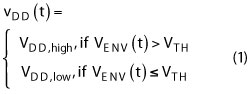
where vDD(t) is an instantaneous drain bias voltage, which has one of the two DC voltages (VDD,low and VDD,high). VENV(t) and VTH are instantaneous output envelope voltage and an output-referred threshold voltage, respectively. If the envelope is greater than VTH, the PA has a drain bias voltage of VDD,high. Otherwise, the bias voltage is instantly switched to VDD,low.
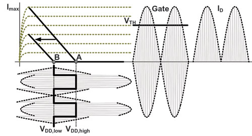
Figure 1 Operation of the Class B PA with a dynamic switching method.
Figure 1 describes the operation of the DDBS on an ideal Class B PA. The envelope signal for the modulated input voltage waveform is compared with the constant threshold voltage. For the envelope signal greater than the threshold voltage, the PA operates at point ‘A’ on the I-V plane and its voltage waveform is presented below the I-V curve. If the envelope level becomes lower than the threshold, the bias point instantly shifts to point ‘B’ so that the voltage waveform also shifts down. The efficiency can then be improved because the DC power consumption is reduced for an envelope signal lower than the threshold.
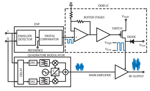
Figure 2 Schematic diagram of the power amplifier with a DDBS IC.
Figure 2 shows a schematic diagram of the power amplifier with a DDBS IC. From the digital I/Q signal, the envelope signal is extracted and is digitized using a digital comparator with a given threshold level. The two-level digitized signal is applied to the DDBS IC and is used to control the switch to select the bias voltage between VDD,high and VDD,low. The DDBS IC is very simple because the envelope signal is processed in the digital domain.
The DDBS IC consists of buffer stages, a switch driver, a PMOS switch and a diode. The buffer and switch driver stages are designed to have rail-to-rail output characteristics in order that the PMOS switch can be fully turned on or off. The size of the PMOS switch and diode should be large enough to drive the required current from the PA. The PMOS switch is designed in consideration of a trade-off between its frequency response and current handling capability. The diode is designed using a native NMOSFET, which has a very low turn-on threshold so that a voltage drop can be low over the diode.
According to the control signal, the voltage VDD,high is supplied to the drain of the PA when the PMOS switch is turned on. The voltage VDD,low is supplied through the diode when the PMOS switch is turned off. The input signal of the PA is the modulated RF signal of which the envelope signal should be accurately synchronized with the dynamic drain bias voltage in time using a time delay block.
One of the most important considerations in the DDBS system design is how to determine the threshold voltage and VDD,low for the best efficiency improvement because VDD,high is generally given by the system. In the next section, the effect of the threshold and VDD,low on the efficiency of the DDBS system will be analyzed. The optimum values for both the threshold and VDD,low will be found.
Operation Conditions
Efficiency of the Class B PA
The threshold voltage gives a reference to bisect and limit the envelope signal, and then composes a control signal for the DDBS IC. Because it is very important to determine the threshold voltage and VDD,low for the performance optimization, they are analyzed based on the ideal Class B amplifier.
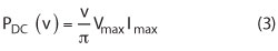
The fundamental output power is given by
where Vmax and Imax are the peak amplitudes of the output voltage and current, respectively. v is a normalized envelope voltage. Thus, v2 is an output power back-off and is defined as Pout/Pmax, where Pmax is VmaxImax/4. The DC power consumption is then given by
Hence, the drain efficiency becomes:
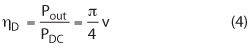
With no output power back-off, where v = 1, the ideal Class B PA has an efficiency of 78.5 percent. If the drain bias continuously varies according to the output power back-off level, the maximum efficiency will be maintained. This condition is given as:

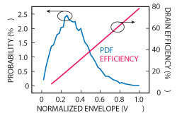
Figure 3 PDF of the up-link 64 QAM OFDM signal and an ideal efficiency of the Class B amplifier according to the normalized envelope voltage.
For the continuous bias modulation methods, such as EER, hybrid EER and ET, Equation 5 is the ideal condition for the drain bias modulation. However, for the DDBS, a single value of VDD,low with the threshold voltage should be selected for efficiency optimization.
Optimum VDD,low and the Threshold Voltage
For the modulated signals such as OFDM, the average efficiency of the PA, rather than the peak efficiency, is meaningful, because the PA operates on a low or mid power region for the greater part of the time. Therefore, statistical distribution of the normalized envelope voltage should be considered to optimize the average efficiency. Figure 3 shows a probability density function (PDF) of the up-link OFDM signal based on the 64-quadrature amplitude modulation (64-QAM). Relatively high statistical distribution can be observed for the normalized envelope voltage between 0.1 and 0.5 V. Figure 3 also plots the drain efficiency of the ideal Class B amplifier.
For the time-varying envelope signals, the average efficiency can be defined as:
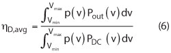
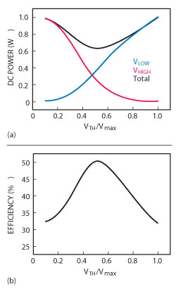
Figure 4 Relative average DC power consumption (a) and average efficiency according to Vth/Vmax (b).
where p(v) is a probability density function of the envelope, Pout(v) is a fundamental output power and PDC(v) is a DC power consumption. The knee voltage of the transistor was assumed to be zero.
The average efficiency of the DDBS system which has two different bias voltages can be expressed as:
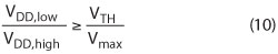
VDD,high is the same as Vmax, due to the zero knee voltage. Pout,avg is an average output power. In order to avoid saturation in the low power region for the linear operation, the following condition should be satisfied:
Here, the maximum efficiency improvement can be achieved if the left and right sides of Equation 10 are the same.
Figure 4 presents the calculated relative average DC power consumption and an average efficiency according to the normalized threshold voltage which is VTH/Vmax. The calculation was done under the condition that VTH is equal to VDD,low for maximum efficiency improvement. If VTH/Vmax is 0, VDD,low and its occurrence are 0 so that only VDD,high is supplied to the drain of the PA. When VTH/Vmax is 1, VDD,low should be the same with VDD,high or Vmax. Therefore, the drain bias has only VDD,high all the time. For both cases, the average efficiencies are approximately 31 percent. The obtained optimum value of VTH/Vmax is approximately 0.52, which means that the VDD,low is 0.52 times VDD,high. The maximum average efficiency is almost 50 percent for the DDBS system.
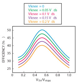
Figure 5 Calculated average efficiency with various knee voltage as a parameter.
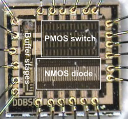
Figure 6 Photograph of the implemented DDBS IC.
For a more practical solution, the knee voltage of the transistor can be considered. It is linear with the drain to source voltage or drain current if a constant on-resistance is assumed. The voltage swing of the fundamental component is restricted by the knee voltage. Calculated efficiencies, with the knee voltages as a parameter, are plotted in Figure 5. A non-zero knee voltage degrades the average efficiency, but the optimum value of VTH/ Vmax is not changed, as shown.
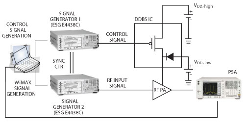
Figure 7 Test setup for the DDBS system.
Experimental Validation
The designed DDBS IC is fabricated using the TSMC’s 0.18 µm CMOS process, with the dimensions of 1×1 mm2, including pads. Figure 6 shows a photograph of the implemented DDBS IC. To verify the feasibility of the DDBS system, the DDBS IC is applied to Anadigics’s AWT6261R, which is a PA for mobile WiMAX application, based on InGaP/GaAs HBT technology. Figure 7 shows the test setup for the overall DDBS system. The upper signal generator provides the DDBS IC with the real-time binary control signal, which is synchronized with the modulated RF signal from the lower signal generator. The binary control signal for the DDBS IC is generated by the PC. The RF modulated signal, which has a center frequency of 2.6 GHz, a bandwidth of 9.4 MHz and a PAPR of 9.6 dB, is applied to the PA.
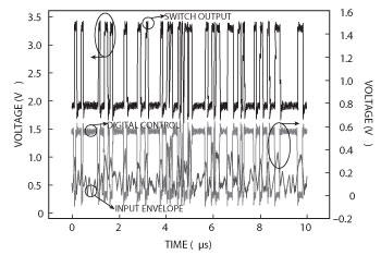
Figure 8 Measured time-domain envelope and its binary control signals for the DDBS IC.
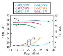
Figure 9 Measured gain and EVM of the power amplifier.
Figure 8 presents the measured results of the DDBS IC with a load resistor of 30 Ω, which is connected to the switch rather than to a PA. Based on the envelope of the OFDM signal, the generated binary control signal is applied to the DDBS IC. VDD,low and VDD,high are 2.0 and 3.3 V, respectively. For this case, VTH/Vmax is approximately 0.45 because a knee voltage of 0.5 V is considered. The measured voltage drop of the diode is as small as 0.08 V.
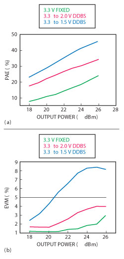
Figure 10 Measured gain and EVM of the power amplifier.
Figure 9 shows the test results of the PA for various fixed drain voltages of 1.5, 2 and 3.3 V. The measured gain is 29.5 dB for the bias voltage of 3.3 V. Gain degradations of 0.6 and 1.6 dB are observed for the supply voltages of 2 and 1.5 V, respectively. The measured EVM performances are almost the same and are approximately 1.2 percent at an output power of 15 dBm. However, the EVM performance is quickly degraded as the output level increases. The lower bias voltage causes earlier degradation in EVM performance due to a signal clipping.
Figure 10 shows the measured PAE and EVM of the power amplifier with the DDBS IC. The measurements were carried out with two different VDD,low voltages of 1.5 and 2 V and a fixed VDD,high of 3.3 V. In order to compose a control signal for the bias switch, VTH/Vmax was experimentally refined from its initial value of 0.52 to 0.45 for the best trade-off between the efficiency and linearity of the DDBS system.
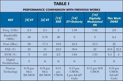
For the DDBS system with a very low VDD,low of 1.5 V, a high PAE of 43.6 percent was achieved with a slightly degraded EVM of 8.4 percent at an average output power of 25 dBm. The degraded EVM could be improved using a digital predistortion technique. However, if the voltage level of VDD,low is slightly increased, the additional circuit for linearity improvement such as digital predistorter is not required. The DDBS system with a VDD,low of 2 V with VTH/Vmax of 0.45 has an increased PAE from 21.3 to 32.28 percent with a good linearity performance, that is an EVM of less than 4 percent, at an output power level of 25 dBm. These performances are compared to the representative previous works in Table 1.
Conclusion
In this article, an efficiency enhancement technique for the power amplifiers based on an DDBS IC is presented. Considering a statistical power distribution of the signal envelope, optimum operation condition of the system is analyzed for the threshold and bias conditions. To verify the performance, the DDBS IC was designed and implemented, using 0.18 µm CMOS technology. It was tested with an InGaP/GaAs HBT PA using the 2.6 GHz band up-link m-WiMAX signal.
The measured results show that a high improvement of PAE by 11 percent was achieved for the VDD,low of 2 V with a good EVM performance of less than 4 percent at an output power level of 25 dBm. The DDBS system has a very simple circuit and provides an effective way to enhance the average efficiency of the PA for the signals having high PAPR.
Acknowledgment
This work was supported by the National Research Foundation of Korea Grant funded by the Korean Government (NRF-2011-220-D00084).
References
- S.C. Cripps, RF Power Amplifiers for Wireless Communications, First Edition, Artech House, Norwood, MA, 1999.
- F.H. Raab, P. Asbeck, S. Cripps, P.B. Kenington, Z.B. Popovic, N. Pothcary, J.F. Sevic and N.O. Sokal, “Power Amplifiers and Transmitters for RF and Microwave,” IEEE Transactions on Microwave Theory and Techniques, Vol. 50, No. 3, March 2002, pp. 814-826.
- G. Hanington, P.F. Chen, P.M. Asbeck and L.E. Larson, “High-Efficiency Power Amplifier Using Dynamic Power-Supply Voltage for CDMA Applications,” IEEE Transactions on Microwave Theory and Techniques, Vol. 47, No. 8, August 1999, pp. 1471-1476.
- F. Wang, D.F. Kimball, D.Y. Lie, P.M. Asbeck and L.E. Larson, “A Monolithic High-Efficiency 2.4 GHz 20 dBm SiGe BiCMOS Envelope Tracking OFDM Power Amplifier,” IEEE Journal of Solid-State Circuits, Vol. 42, No. 6, June 2007, pp. 1271-1281.
- J. Chen, K.U. Yen and J.S. Kenny, “An Envelope Elimination and Restoration Power Amplifier Using a Dynamic Power Supply Circuit,” 2004 IEEE MTT-S International Microwave Symposium Digest, pp. 1519-1522.
- Y. Li, J. Lopez, D.Y.C. Lie, K. Chen, S. Wu, T.Y. Yang and G.K. Ma, “Circuits and System Design of RF Polar Transmitters Using Envelope-Tracking and SiGe Power Amplifiers for Mobile WiMAX,” IEEE Transactions on Circuits and Systems, Part I, Regular Papers, Vol. 58, No. 5, May 2011, pp. 893-901.
- C.J. Li, C.T. Chen, T.S. Homg, J.K. Jau and J.Y. Li, “High Average-Efficiency Multimode RF Transmitter Using a Hybrid Quadrature Polar Modulator,” IEEE Transactions on Circuits and Systems, Part II, Express Briefs, Vol. 55, No. 3, March 2008, pp. 249-253.
- C. Buoli, A. Abbiati and D. Riccardi, “Microwave Power Amplifier with Envelope Controlled Drain Power Supply,” 1995 European Microwave Conference Digest, pp. 31-35.
- A. Khanifar, N. Maslennikov, R. Modina and M. Gurvichm, “Enhancement of Power Amplifier Efficiency Through Dynamic Bias Switching,” 2004 IEEE MTT-S International Microwave Symposium Digest, pp. 2047-2050.
- Y.S. Jeon, J. Cha and S. Nam, “High-Efficiency Power Amplifier Using Novel Dynamic Bias Switching,” IEEE Transactions on Microwave Theory and Techniques, Vol. 55, No. 4, April 2007, pp. 690-696.
- A. Shameli, A. Safarian, A. Rofougaran, M. Rofougaran and F.D. Flaviis, “A Two-Point Modulation Technique for CMOS Power Amplifier in Polar Transmitter Architecture,” IEEE Transactions on Microwave Theory and Techniques, Vol. 56, No. 1, January 2008, pp. 31-38.
- A. Kavousian, D.K. Su, M. Hekmat, A. Shirvani and B.A. Wooley, “A Digitally Modulated Polar CMOS Power Amplifier With a 20 MHz Channel Bandwidth,” IEEE Journal of Solid-State Circuits, Vol. 43, No. 10, October 2008, pp. 2251-2258.\
- J.S. Walling, S.S. Taylor and D.J. Allstot, “A Class-G Supply Modulator and Class-E PA in 130 nm CMOS,” IEEE Journal of Solid-State Circuits, Vol. 44, No. 9, September 2009, pp. 2339-2347.
- J. Choi, D. Kang, D. Kim and B. Kim, “Optimized Envelope Tracking Operation of Doherty Power Amplifier for High Efficiency Cver an Extended Dynamic Range,” IEEE Transactions on Microwave Theory and Techniques, Vol. 57, No. 6, June 2009, pp. 1508-1515.
- C.D. Presti, F. Carrara, A. Scuderi, P.M. Asbeck and G. Palmisano, “A 25 dBm Digitally Modulated CMOS Power Amplifier for WCDMA/EDGE/OFDM With Adaptive Digital Predistortion and Efficient Power Control,” IEEE Journal of Solid-State Circuits, Vol. 44, No. 7, July 2009, pp. 1883-1896.