
Tremendous changes are occurring in the area of wireless communications, so much so that the mobile phone of yesterday is rapidly turning into a sophisticated mobile device capable of more applications than PCs were capable of only a few years ago. For example, the data rates provided by the initial High Speed Downlink Packet Access (HSDPA) extension to 3G networks enable a user to wirelessly access the Internet at speeds up to 1.8 MBits/second. Further enhancements in HSDPA modulation schemes will soon increase this speed to greater than 10MBits/second. So downloading your latest e-mails with a 5 MB Powerpoint™ attachment outside of the office is no longer a frustrating and time-consuming exercise. In fact, it is just as fast as when you are in the office.
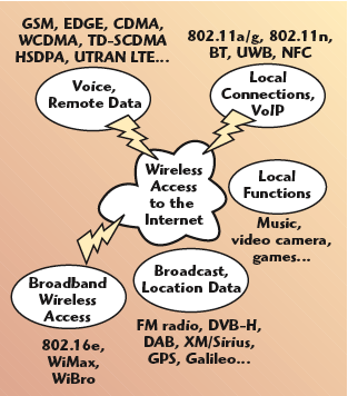
It is the need and desire of people to access the Internet from anywhere in the world that is driving many of the new changes that are occurring in the largest consumer market ever — the wireless mobile device market. In Figure 1 we look at the mobile device view and see that there are three main routes to wirelessly access the Internet. Voice is still the main use of mobile devices and the GSM and CDMA networks around the world now connect over 2.3 billion wireless subscribers. The cellular standards are evolving to add high speed data connections, and cellular remains the way we connect from remote locations many miles away from a base station.
For local connections Bluetooth“ is rapidly becoming a common feature in mobile devices with almost 30 percent attachment rate expected in 2006. This attachment rate is expected to grow to more than 50 percent over the next three years. Today we are seeing other radios being combined with Bluetooth, such as WiFi, FM radio and Near Field Communications (NFC). Soon we will see combination Bluetooth and Ultra-wideband (UWB) devices to further enhance the wireless distribution of multimedia content. It will not be long before that 5 MB presentation will be beamed to an UWB-enabled plasma monitor in the conference room or displayed directly in real time onto your colleagues’ mobile device at the table.
The third area being developed for wireless access to the Internet is the evolution of mobile broadband. Worldwide Interoperability for Microwave Access (WiMAX) is an industrial organization that promotes the 802.16 standard for both fixed and mobile devices. WiMax uses frequency bands between 2 and 11 GHz and does not require a line of sight between base stations. Each WiMax base station will theoretically have a range of about 30 miles. It is likely that WiMax will be used initially as a wireless alternative to DSL cable, especially in rural areas where the cable infrastructure is not very well developed. In 2007 it is likely that mobile WiMax will be built into laptops, similar to WiFi today, shortly followed by implementation into smart phones. Sprint is already preparing networks, and Motorola is planning to supply the devices.1
In addition to the ability to wirelessly access the Internet the mobile device of tomorrow will also be capable of viewing TV programs, watching videos, storing and playing music as well as providing location-based services using GPS or Galileo satellite navigation systems.
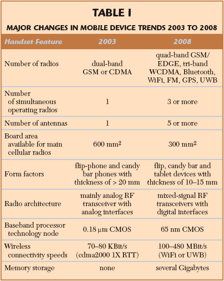
Major Changes in Mobile Device Trends
The More Radios the Better
Major changes are occurring in the mobile device arena in terms of radio complexity, as illustrated in Table 1. Firstly, the number of radios being designed into mobile devices is increasing. Just a few years ago the only radios needed were dual-band (800/1900 or 900/1800 MHz) GSM or CDMA. We project that in 2008 it will be common to have as many as seven radios inside mobile devices. The major shift is the addition of HSDPA as more 3G phones become available. In order to satisfy the requirements of global networks, it is likely that the 3G radio will be at least tri-band covering regions 1, 2 and 5, followed by the need for several other regions. Adding different regions for WCDMA or HSPDA is more complicated than previously because each frequency pair needs a duplexer to separate the transmit and receive signals that are active at the same time. Bluetooth, WiFi, FM, GPS and DVB-H are the other five radios that are expected to be added in the next two years. Looking at the usage models suggests that many of these radios need to be capable of simultaneous operation, so interference and co-existence must be considered early in the design. For example, the US band of 800 MHz has a second harmonic that is right on top of the 1600 MHz broadcast TV channel used by Modeo for DVB-H (Digital Video Broadcast-Handhelds). Therefore, filtering must be designed so as not to block the TV viewing experience when you are talking on the phone, something that will soon be a common use of mobile devices.
Antennas Everywhere
All these radios will have different antennas requiring careful partitioning of the radios so that the antennas can be placed in optimal locations inside the mobile device and positioned such that interference is minimized. Another significant factor affecting mobile devices is that as the antennas become more broadband their impedance match degrades and the cellular power amplifier has to deliver power into a higher VSWR load. The antenna VSWR also changes significantly as the mobile device is placed near objects such as the body, metallic objects, inside briefcases, etc., and the power amplifier has to accommodate the changing environment to maintain the expected performance of total radiated power (TRP). Developing load insensitive power amplifiers and adaptive matching networks are key to maintaining the best user experience.
Shrinking Real Estate
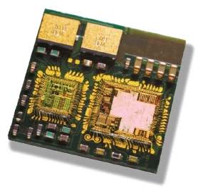
Another trend happening inside a mobile phone is the reduction of space available for the radio. Phones are being designed that are thinner, slimmer and narrower than ever before. Only a few years ago the space available for the total RF section in a dual-band GSM or CDMA phone was close to 600 mm2. Now the space available for a 3G phone with multiple GSM, EDGE, HSDPA radios is half that at only 300 mm2. This trend has led to more and more integration of components both at the silicon level and at the module level. For example, nowadays VCOs, synthesizers loop filters and voltage regulations are all integrated into the transceiver die. Additionally, SAW filters (see Figure 2) and in the future, crystal reference oscillators, are being incorporated into the transceiver module to realize a complete, self-contained system module in a small package.
The trend now is for very thin phones, with some now less than 10 mm thick. This implies that phone manufacturers desire to use only one side of the printed circuit board whereas before both sides were utilized. This also puts pressure on component manufacturers to shrink the size of the solutions. In the future we predict that mobile devices will be designed with more interesting form factors, including flexible materials for clothing and other applications. So making the components as small as possible is a key requirement for realizing almost all new devices.
Going Digital
Traditional RF architectures have usually been implemented using mainly analog approaches for downconversion, modulation and filtering. In recent years there have been advances in design and process technologies that have allowed the conversion from RF to digital to occur within the radio before the baseband. For example, in RFMD’s POLARIS™ TOTAL RADIO™ the transceiver uses a fractional-N synthesizer-based digital GMSK and 8PSK modulator all implemented in digital CMOS. This has also helped realize digital interfaces between the RF and baseband sections of the radio that allows the baseband chip to migrate to smaller and smaller CMOS geometries and segments the analog and mixed-signal elements into the front-end.2
In other developments even more integration of the RF functionality has been implemented in a digital fashion, an example of which is the Bluetooth“ chip from Texas Instruments.3 It remains to be seen how widespread this type of architecture will be adopted in the cellular handsets. Already similar ICs are available for the low end GSM standards but it will likely be several years until it is seen in 3G handsets. However, the trend is definitely towards more digital content in the radio.
Cellular Handset Functional Blocks
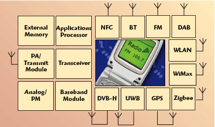
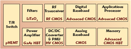
Whereas there are always some differences between standards and tiers, in general the semiconductor-based functional blocks of a mobile device are as shown in Figures 3 and 4, with representative technologies shown. Of course, many other technologies can be used, but these shown are the most common. These are generally categorized into the following:
• Front-end components
a.) T/R and Mode Switch
b.) Power Amplifier
c.) RF Transceiver
d.) Filters, both Rx and Tx
• Communications Processor (baseband)
• Applications Processor
• Power Management and Analog Baseband
• Peripherals

Many excellent choices exist today for high performance semiconductors used in consumer devices. Computer and memory markets tend to drive the state-of-the-art for deep submicron digital CMOS, while the mobile phone market is the volume driver for mixed-mode and analog semiconductor processes. Historically, the RF and analog front-end has been optimized by function, with very little integration. The RF and analog front-end components are defined herein as all semiconductor blocks between the antenna and the digital baseband, non-inclusive. These functions were initially implemented as discrete solutions, on the phone board. In recent years the discrete solutions have been replaced with more integrated solutions — on-chip integration in some cases, module integration in others. Either way, the goal was to reduce the component count on the phone board and to enable new, lower cost and higher performance “super-components.”
The trend toward module integration has allowed each function to continue to be optimized by semiconductor technology. For example, a GSM transmit module today consists of a PA, matching components, bandpass/low pass filter and transmit/receive switch. Generally speaking, the PA is either GaAs HBT or Si LDMOS, the match and filters are implemented as discrete SMD components and in some cases microstrip lines on the module substrate, and the transceiver switch is GaAs pHEMT. An example is shown in Figure 5. These choices of technologies allow the function to be implemented with minimal performance compromise.
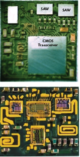
Transceivers are also moving toward integrated solutions, with CMOS clearly becoming the preferred technology. Performance is very competitive, and the cost roadmap for CMOS is unparalleled due to the economies of scale driven by the digital markets. Solutions for the front-end of a GSM/EDGE phone combine on-chip integration and module integration for the optimum tradeoff between cost and performance. Today, a two-module solution exists for the entire cellular front-end, as shown in Figure 6. This allows the phone manufacturer much simpler and lower cost design and manufacturing while shifting the burden of designing these components to the component supplier.
Technology Partitioning
As was mentioned earlier, some suppliers are integrating the RF transceiver together with the digital baseband as a system-on-chip (SoC). This allows the transceiver, which is migrating toward more digital processing techniques, to take advantage of the digital CMOS “platform.” In this case, the remainder of the front-end is left to discrete or module-implemented solutions.
These solutions merge RF, analog and digital circuitry on a single CMOS process, which provides a single low cost platform to build upon. The trend is interesting, but as the advanced CMOS geometries continue to shrink, it will be difficult to maintain due to two reasons:
1. Analog voltages such as those needed for I/Os, LDO regulators, DC-DC converters, charge pumps for micro-electromechanical systems (MEMS) and other power management functions will not be supported. This will drive the power management into a separate technology, and will be required as part of the chipset.
2. As integration in the front-end occurs, technology will drive the partitioning toward digital-only in deep submicron CMOS and RF/analog in a higher voltage CMOS process. MEMS will reside here as well, to complete the front-end integration. This front-end integration platform will be a key for reducing cost and size, and enabling adaptability.
Integration drives cost and performance, so ultimately a highly integrated single-chip solution will be the most cost-effective means to produce the front-end. Technologies are being developed to address this need, and within the next few years, we will see new technologies drive new architectures, most likely on a CMOS-based technology platform.
Battery Technology Trends
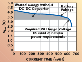
Power requirements for mobile phones continue to increase due to larger color displays, additional radios, new standards for high speed data, etc. This places a greater demand on the battery, requiring ever-increasing energy densities. One way battery manufacturers are responding is by defining new materials to extend the useful life, but to the component manufacturer this typically means a greater range of supply voltage. For example, Figure 7 shows the typical discharge curve for Li-Ion technology. Newer technologies allow extended talk time, but require operation to a lower voltage — as low as 2.5 V.
Most components are driven by voltage regulators or DC-DC converters contained within the power management IC. Digital chips require typically 1.8 to 1.3 V, which must be efficiently converted from the 4.2–2.7 V battery. RF transceivers typically do not consume a significant amount of current; thus, their power consumption is minimal over the discharge curve and their voltage can be supplied with a low dropout regulator (LDO). The power amplifier is typically the largest consumer of power, next to the baseband and/or display, so various means to improve power amplifier efficiency are employed.
Increases in Power Amplifier Efficiency
The DC power used by the power amplifier (PA) is converted either into RF power and transmitted to the antenna, or dissipated into the phone board and converted to heat. Efforts are made to minimize the wasted power, and to optimize the percentage converted to RF energy. Several techniques include:
Optimizing the Semiconductor Technology Used for the PA
The core efficiency of the PA is limited by the knee voltage (sometimes referred to as saturation voltage) of the semiconductor device. In order of decreasing efficiency, GaAs pHEMT, GaAs HBT, SiGe HBT and Si LDMOS are the technologies currently in use for mobile phone applications, with GaAs HBT having the largest share by far.
The load impedance, which defines the amount of power available and the efficiency of the PA, is set both by the knee voltage and the supply voltage (Vbat), as shown in Equation 1. For a varying supply voltage such as a battery, the load must be set to provide the required power at the minimum voltage available. Then for a fixed load, whenever the battery is not at its minimum voltage level (fully discharged), the additional voltage headroom is wasted as heat

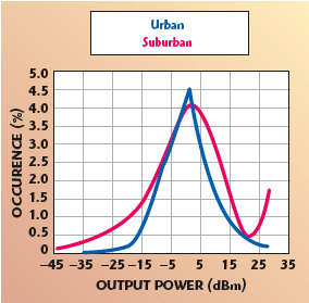
In some applications the load impedance is modified at a reduced power level to re-optimize the PA at that lower power. This has the effect of improving efficiency at that power. For a system such as IS-98 (US-CDMA), this can have a dramatic effect on the total talk time of the phone, as the power level from the phone is typically centered around 0 to 5 dBm (see Figure 8).
Reducing the Post-PA Losses, Which in Turn Minimizes the Amount of Power Required From the PA Device Itself
These losses arise from the matching network for the amplifier as well as the switching network required at the antenna. Clever architectural choices can help reduce losses, but options are somewhat limited in multimode environments where multiple signals must be switched to the antenna(s).
Recovering Lost Power
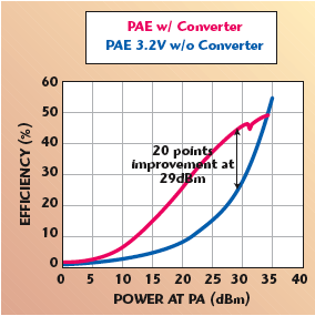
As shown in Equation 1, the minimum battery voltage determines the load impedance to provide a given power. Lower minimum voltages means more wasted power when operating at any point above the minimum. As can be seen from the figure, this can mean a significant amount of wasted power. If the voltage can be efficiently converted from the battery voltage to the required operating voltage for the PA, then that wasted power can be recovered. DC-DC buck converters perform this task, although they are just being developed for some higher power PAs, such as for GSM systems. The advantage is shown in Figure 9, where the efficiency of the system is improved at reduced power levels by the DC-DC converter.
New trends in battery technologies are driving toward greater voltage range to achieve longer talk times, with minimum voltages as low as 2.5 V. Referring to Equation 1, as Vbat is reduced so is RL, impacting total efficiency. Some technologies are better optimized for low voltage operation, such as GaAs HBT and GaAs pHEMT due to their lower Vknee. Ultimately, a boost DC-DC converter for the PA should provide the best talk times, as the PA is optimized for a higher RL and the total energy from the battery is conserved even at higher voltages.
The improvement shown in Figure 9 can be seen for a constant-envelope modulation system like GSM/GPRS. For a linear system, such as EDGE, the transmitter must support higher peak powers due to the amplitude modulation involved. Generally, these systems are implemented with an I/Q modulator and a linear transmitter, but this requires the PA to be backed off from saturated power, which reduces efficiency. A PA will typically achieve > 55 percent peak efficiency in GSM, but only ~20 to 25 percent in linear EDGE mode. This places severe constraints on the phone, not just from a talk time perspective, but also from heat dissipation. Some EDGE systems are implemented using polar modulation, which uses phase and amplitude modulation directly on the PA. In this system, the PA operates in saturation, just as in a constant envelope system like GSM. The phase modulation is applied to the RF input while the amplitude modulation is applied to the voltage supply to the PA. If the amplitude is modulated with a high speed DC-DC converter (which can support the required EDGE bandwidth), the transmitter can operate with efficiency close to a GSM transmitter while maintaining the linear operation needed for EDGE. These innovations will continue with new systems (OFDM-based schemes being considered for 4G, for example).
Other techniques for preserving efficiency at backed-off powers include phased power combining approaches like Doherty and Chirex, and these are being implemented in some forms today. However, they do not address improved efficiency versus battery voltage.
Coping with Antenna Mismatch
As mobile phones have shrunk in form factor, so have the antennas. What used to be a nice (from a RF design perspective), long, retractable dipole antenna is now a very small patch antenna supporting multiple bands and standards, and incorporating acoustic cavities and speakers. The susceptibility of these antennas to proximity effects is much higher, and this translates to higher VSWR at the transmitter. For linear systems, isolators used to be common to maintain a constant PA load impedance into a VSWR, but are no longer used. Nonlinear systems such as GSM suffered power and gain variation, translating to significant efficiency reductions with VSWR. Techniques to maintain performance, both for linear and nonlinear systems, are now in place, and more innovative solutions are being developed. These can be passive using phased power combining networks, or active using digitally controlled tuned load networks.
Passive phased networks work by combining the forward power from two PAs in phase, but canceling reflected power by combining out-of-phase. New techniques are in development to allow dynamic tunability of the load impedance, which can adapt to VSWR as well as changes in power level and/or battery voltage as well. Adaptive tuning requires some kind of structure that can modify the elements in the matching network, typically capacitors. Examples include barium strontium titanate (BST) capacitors that can be varied through an analog DC voltage, and MEMS-based switched capacitors that offer digital tuning capability for the load network.
RF MEMS
RF MEMS offers the potential to revolutionize the multimode radio front-end. The lower loss associated with above-IC MEMS switches and the possibility of tunable resonators can be used to integrate much of the functions currently performed by external, specialized substrates and technologies. In addition, they should provide improved functionality and performance, including tunability to enable operation in a multi-standard environment, leading to a truly cognitive radio.
RF MEMS switches have begun appearing on the market with reported reliability > 1E10 switching cycles and switching speeds < 10 ms, and carrying losses of < 0.2 dB with isolation > 40 dB at 2 GHz. This level of performance is sufficient to enable use in a multitude of applications, beginning with transmit/receive switching for GSM. The inherent linearity of a mechanical switch allows for WCDMA mode switching without distortion and with very low losses. Additional modes and/or radios sharing antennas can be switched very easily using MEMS switches. Above IC processing allows the MEMS devices to be built directly on CMOS, allowing control for the switch to be integrated in silicon (Si), but also to allow the MEMS devices to be integrated with other analog functions in CMOS.
Other applications for MEMS devices include crystal replacements for reference frequency generation. Some commercial products are beginning to emerge; however, the stability required to meet GSM phase noise is not yet available. These products are improving, using state-of-the-art silicon-on-insulator (SOI) technologies and/or above-IC beam resonators, and will soon be capable for all standards. Once integrated, opportunities for multiple frequencies exist, selectable with on-board MEMS switches, or perhaps by a bias voltage directly.
Using RF MEMS resonators for RF filtering can provide very compact, tunable, front-end filtering for multiple standards and/or frequencies. These resonators have been plagued by high motional resistance, limiting the capability to couple energy and thus causing very high losses in 50 Ω systems. Research is ongoing, however, to reduce the motional resistance, and to keep the quality factor (Q) high in the resonators. These devices will ultimately provide the front-end for a multi-standard, multi-band radio; the tunability will allow a feasible software-defined radio (SDR), with some amount of channel selection at the front-end.

Alastair Upton
Conclusion
The tremendous changes occurring in wireless communications are driving the mobile device to incorporate more radios inside the handset, while shrinking the physical size. This dynamic leads to innovative solutions to maintain electrical integrity while more than one radio is operating simultaneously, and to integrate more functionality into smaller packages while maintaining good thermal properties. But these are challenges that engineers thrive upon. Because we are creating the mobile phone of the future, or more correctly, the mobile device of the future, that will have more functionality than even some laptop computers have today.
References
1. Future Mobile Handsets: Worldwide Market Analysis & Strategic Outlook, Seventh Edition, Informa Telecoms & Media, pp. 572–574.
2. B. Wilkins, “The Benefits of Standard Radio-to-Baseband Digital Interfaces,” High Frequency Electronics, July 2003, pp. 38–40.
3. R.B. Staszewski, et al., “All-Digital TX Frequency Synthesizer and Discrete-time Receiver for Bluetooth Radio in 130-nm CMOS,” IEEE Journal of Solid-State Circuits, Vol. 39, No. 12, December 2004, pp. 2278–2291.

Victor Steel
Alastair Upton holds a BSc (Hons) degree in electrical engineering from the University of Leeds (UK) and an executive master’s degree in technology management (EMTM) from the University of Pennsylvania/Wharton School of Business. He is managing director of strategic marketing for the cellular business at RFMD. Prior to this role, he was general manager of the digital cellular product line, responsible for initiating the Polaris™ TOTAL RADIO™ chipset products. He has been with RFMD since 1997 and has held product line director and product manager positions within the company. Prior to joining RFMD, he was with Lockheed Martin/GE Aerospace for 14 years as program manager, engineering manager and GaAs integrated circuit designer. He started his career with Philips in 1980.
Victor Steel received his MSEE degree from the University of Illinois in 1987. He is RFMD’s vice president of corporate research & development (R&D). Previously, he served as director of RFMD’s power amplifier product line from its inception until May 2000, when he formed the R&D group. Prior to the formation of product lines, he served as engineering manager for all of RFMD’s power amplifier product development. Before joining RFMD in 1993, he was employed by ITT GaAs Technology Center in Roanoke, VA, as a senior design engineer, developing commercial power amplifier products as well as managing the test lab for the wafer fab.