
An ultra-wideband (DC to 125 GHz) nonlinear model for a W-Band Schottky diode is presented in this article. The model is validated against multiple measurement datasets, including IV and S-parameters at different bias and temperature conditions. Its large signal performance is studied against large signal harmonic power measurements to illustrate its capability to accurately predict the device’s nonlinearities, such as harmonic levels.
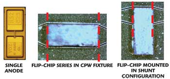
Figure 1 A single anode Schottky diode along with two test fixtures setups.
Schottky diodes are widely used as detectors or mixers in transceiver modules due to the low forward voltage drop and very fast switching speed. This is the result of the device structure – a metal layer deposited on semiconductor material such as GaAs and SiC, forming the “Schottky barrier.” In this work, an advanced ultra-wideband nonlinear diode model that covers the DC to 125 GHz frequency range for a W-Band Schottky single anode diode from Virginia Diodes Inc. is described.1 Although there have been models of sub-mm wave and THz Schottky diodes in the literature in the past,2 this is the first known model that is based on and validated against such broadband data and implemented in multiple commercial simulation platforms.
To develop and fit appropriate package parasitic and nonlinear modeling elements, custom fixturing was developed. The fixturing used 10 mil quartz coplanar-waveguide lines, along with custom calibration standards that enabled reliable ultra-broadband bias dependent data for the Schottky to be obtained. Figure 1 shows the top view of the diode as well as the series and shunt “flip-chip” configurations used. The red lines illustrate the reference planes of the measurement. Measurement-related specifics of this work are described elsewhere.3 The model was developed based on series measurement datasets, including DC I-V, C-V, R-I and S-parameter measurements over temperature (25° and 85°C). Anritsu’s Vector Star ME7838A mm-wave VNA was used to obtain the broadband S-parameters, ranging between 70 KHz and 125 GHz. While the internal details of the model are proprietary, encoded models fully compatible with popular microwave circuit simulators are now commercially available for both a single-anode and a zero-bias detector diode.4 A review of example model performance for the single-anode W-Band Schottky diode is outlined briefly in the following sections.
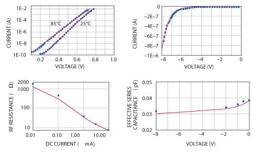
Figure 2 DC I-V, R-I and C-V measurements (markers) and simulations (solid lines).
Study of Model Performance
Figure 2 shows the measured DC I-V, R-I and C-V data, compared with the model. As can be seen, the model predicts all these measurements well and shows good temperature scalability. The R-I curve shows that the junction resistance decreases exponentially as the diode becomes more conductive. Cj increases gradually with the decrement in the reversed bias voltage (up to 0 V). The RF resistance and effective capacitance versus bias data, for model extraction, was obtained from the measured S-parameters. An accurate low frequency core model was achieved by fitting to the R-I and C-V data at 1 GHz. As illustrated, the developed model captures the nonlinearities in Rj and Cj very well. This sets the stage for a robust broadband model after carefully applying a high frequency parasitic treatment.
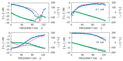
Figure 3 Multi-bias broadband S-parameters comparison between measurements (markers) and simulations (solid lines).
Figure 3 shows the S-parameters comparison between the measurements and simulated results at multiple bias conditions. The transition in the diode conduction can be seen in the magnitude in S21. The model accurately predicts the S-parameters (magnitude and phase) from DC up to 125 GHz. The resonance in the S11 around 100 GHz for 0.1 mA bias condition is correctly captured, a result of careful package/parasitic effect modeling.
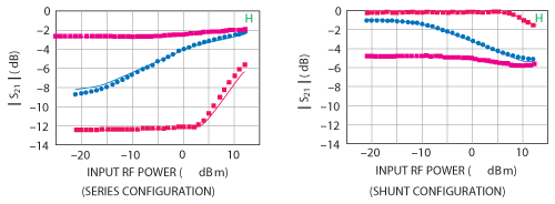
Figure 4 S21 comparison between measurements (markers) and simulation (solid lines).
Large signal power sweep measurements were taken on the Schottky diode at 10 GHz. The model is simulated to compare to the nonlinear datasets. Figure 4 shows the gain compression (that is S21) comparison for the series case at different bias conditions in the two setups (red = 0 V, blue = 0.1 mA, pink = 10 mA). As expected, in series configuration, when the diode conducts (1 mA), the insertion loss (S21) is low, meaning the power going to the output load; whereas for shunt configuration, most of the signal power goes through the diode to ground, leading to higher loss in S21. The model predicts the trend of the S21 versus input power very well for all conditions. Harmonic power data comparisons, not included here due to space limitations, also show excellent agreement.
Conclusion
An ultra-wideband nonlinear diode model, for a W-Band Schottky diode, has been developed, that demonstrates excellent performance in predicting both the small signal and large signal behavior of the diode under test. The excellent large signal performance that the model illustrates is the result of careful treatment of the IV, R-I and C-V nonlinearities of the diode. A separate model was developed for a W-Band zero-bias detector (ZBD) diode, for which comparable performance was achieved in accurately predicting the measurement results of the actual device. This study results from a practical modeling approach, based on measurements and the equivalent circuit model for W-Band Schottky diodes.
References
- See the single anode datasheet at http://vdi.bz/diodes.
- B.L. Gelmont, D.L. Woolard, J.L. Hesler and T.W. Crowe, “A Degenerately-doped GaAs Schottky Diode Model Applicable for Terahertz Frequency Regime Operation,” IEEE Transactions on Electron Devices, Vol. 45, No. 12, December 1998, pp. 2521-2527.
- L. Dunleavy, “Ultra-Broadband Characterization of Schottky Diodes,” appeared in the June 2012 Automatic RF Techniques Group Conference Digest.
- Model downloads can be requested at www.modelithics.com/mvp/VDI/.