
Commercial applications of phased-array antennas have been extensively studied over the last decade, principally in the case of vehicular antennas. Beside the problems related with the design of such an array, there are some general considerations that must be taken into account. If the vehicular antenna has a high gain, tracking the satellite while following both vehicular and orbital motions is difficult and expensive. If the vehicular antenna has a low gain, the capacity of the communications link is limited. However, in the case of a vehicular terminal, the antenna geometry must have a low profile contour, making difficult the efficient use of the antenna aperture.
| |||||||
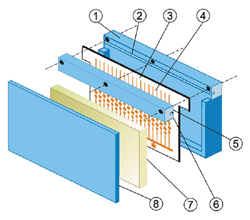
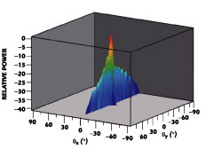
In the frame of the multi-segment System for Broadband Ubiquitous Access to Internet Services and Demonstrator (SUITED)1 project, a phased-array antenna has been designed with the ability to scan the beam over a certain angular range, especially at very low elevation angles (see Figure 1). SUITED is funded by the European Union under the Information Society Technologies (IST) program, aiming to make a significant contribution towards the understanding and development of IP-based mobile networks, consisting of both satellite and terrestrial (UMTS, GPRS, W-LAN) components.
All the antenna parts were realized and measured, and their predicted performances were achieved. The antenna is fully integrated. The methods for adjusting amplitude and phase of each antenna element were also developed, including auxiliary hardware compatible with the standard antenna control board and auxiliary software for parameter settings. The methods were successfully tested in an anechoic chamber. Flexibility in adjusting phase and amplitude characteristics enables optimization of the radiation pattern.
Terminal Architecture
According to the Alenia-Spazio link-budget for the ITALSAT satellite network, the basic requirements for a low communication rate of 256 kb/s were for the receiver, G/T = 3.1 dB/K at K-band (f = 19.78 GHz) and for the transmitter, EIRP = 38 dBW at Ka-band (f = 29.97 GHz). At the same time, the elevation objective was to cover the range from 32° to 48°. From the point of view of the overall dimension of the terminal the main target was to design a phased-array antenna competitive with a parabolic antenna of 30 dB gain. The antenna tracking was determined to be electronic in elevation and mechanical in azimuth.
In the process of producing a functional model of the terminal, it was found more suitable to use a segmented approach to the design.2 Two separate antennas have been designed for transmission and reception. The antenna configuration is based on the use of inclined elementary sub-arrays. Despite the esthetical aspect of a completely flat antenna, an inclined antenna array has an advantage because the antenna's maximum radiation points towards the desired scan range. The inclination and mutual distance of the sub-arrays were calculated to minimise blockage of the array placed in front3 and to prevent the appearance of high level grating lobes within the scan range.4
As shown in Figure 2, the antenna consists of two platforms — movable and stable. The microwave components for the transmitting and receiving antennas (RF TX and RF RX), the control boards for transmitting and receiving antennas (CB TX and CB RX), and the protection circuit for the power supplies of the transmitting and the receiving antennas (PC RX and PC TX) are attached to the movable platform. The stable platform consists of the main power supply, main control board, microwave multiplexer, step motor and optical encoder.
| |||||||
The microwave components of the transmitting antenna consist of the radiating elements, power amplifiers, driver amplifiers, phase shifters and a power divider. The microwave components of the receiving antenna are the radiating elements, low noise amplifiers, high gain amplifiers, phase shifters and a power combiner (see Figure 3).
| |||||||
The control circuit for the transmitting antenna generates voltages applied to the control pins of the transmitting phase shifters. The power control circuit enables appropriate voltages at the gate and drain connectors, and suitable time sequences for drain and gate voltages to switch on and off. The control circuit for the receiving antenna generates the voltages necessary for the receiver phase shifters. The processor included in this board also communicates with the main control board over the VHF communication line.
The power control circuit for the receiver antenna stabilizes the voltages necessary for the receiver and high gain amplifier, and enables the time sequences necessary for amplifier protection. The two platforms are connected with the microwave rotary joint, a VHF capacitive coupler and a DC rotary joint with brushes.
The main control circuit communicates with the external processor over a serial communication line and with the movable platform with an FM, VHF communication line. It generates data for control voltages according to the required beam position and generates sequences for the step motor according the data received from the pointing acquisition tracking (PAT) and the shaft encoder. The main power supply is a DC/DC converter, intended to provide efficient voltages for the main power consumption and protect the terminal from ordinary short circuit faults.
Transmitter Antenna Description
The transmitter radiating elements are realised as passive structures. The sub-array includes four groups of eight printed dipoles. The impedance of each dipole is designed such that the serial connection of eight radiating elements shows satisfactory return losses without any additional matching circuit.5 The dipoles are fed with symmetrical microstrip lines and the outputs of each unit of eight dipoles are combined with balun transitions made by tapering the microstrip line,6 as shown in Figure 4. The output of each sub-array is connected to a high power amplifier.
| |||||||

The power amplifier is made of two MMICs with 1 dB gain. The overall gain of the power amplifier is 30 dB. The maximum output power is 28.5 ±1 dB. At saturation, this power can increase to 1 W (30 dBm).
The gain of the driver amplifier is 20 dB and its maximum output power is 20 dBm. The gain of those amplifiers depends on the gate voltage. By applying high negative gate voltage, the gain of amplifiers can be decreased down to –40 dB (high isolation). This effect is used to exclude certain sub-arrays during the measurement and adjustment of phase and amplitude characteristics.
The phase shifter shown in Figure 5 is realized as an IQ modulator. The 90° power divider is made of a branch line coupler and the in-phase adder uses a Wilkinson divider fabricated on an alumina substrate. Hittite HMC292 mixers are used as biphase attenuators. The insertion losses of the phase shifters are between 14 and 18 dB. Fortunately, the transmitter amplifier operates in saturation and a 4 dB amplitude imbalance is not critical because the AM/PM conversion causes a relatively negligible phase distortion (up to 6°).
|

In order to overcome the losses in the integrated power divider, it includes two stages of packaged medium power amplifiers, HMC 263 LM1 (from Hittite), as shown in Figure 6. The input signal is amplified by the high gain amplifier and divided four ways. The losses in the first divider are 8 dB at 30 GHz. The output ports are fed to the same amplifiers with 20 dBm of output power. After the 7 dB losses in the second divider, the average output power at the divider output is 13 dBm.
|

Receiver Antenna Description
A similar concept of antenna array has been applied to the receiver. The receiving antenna sub-array (see Figure 7) consists of 32 printed dipoles backed with a metal reflector placed a quarter wavelength away at the center frequency. Each sub-array is directly connected to the input of a low noise amplifier (LNA). The design of the LNA was carried out using NEC32584 transistors. The NF measured at 20 GHz was 2 dB with a gain of 10 dB.
|
The high gain amplifier is identical to the driver amplifier in the transmitter chain. The high isolation performance, when a gate voltage below pinch-off is applied, is used to switch off a particular sub-array. The strongly dependent gain versus gate voltage is used for amplitude balance between sub-arrays to suppress grating and side lobes.
The realization of the receiving phase shifter is identical to the transmitter phase shifter. The main difference is in the control logic. Because of the fact that the receiver works in a linear regime, applied voltages to the I and Q ports must enable phase changes with minimum amplitude variation. For this reason, analog voltages are applied to the I and Q ports. These voltages are also adjusted to compensate imbalances in the amplitude and phase characteristics between the sub-arrays. The minimum losses, which enable a flat amplitude characteristic, are 18 dB. The complete receiver chain is shown in Figure 8.
|

The receiver power combiner, shown in Figure 9, is realized in a similar manner, as was explained in the case of the transmitter antenna. The losses in the power combiner are 3 dB. At the output port, an additional high gain amplifier is added for loss compensation.
|
The rotating platform includes the microwave diplexer and rotary joint system. The diplexer is made as a simple T-junction of two coupled line filters corresponding to the transmit and receive bands. The loss in the diplexer is less than 3 dB and the isolation is greater than 35 dB. The loss in the rotary joint is less than 2 dB. Around the microwave rotary joint, a ring with brushes is used to connect the DC power. A capacitive ring at VHF is used to transmit the FM modulated control signal from the main control board to the control board on the movable platform.
Rotating Platform
| |||||||||||||
|

The signal generated at the main control board is a 20 dBm, 100 MHz, FM signal. This signal is received at the receiver control board by an integrated FM receiver with –60 dBm sensitivity. The attenuated level of the received control signal after the capacitance ring is –20 dBm.
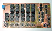
According to the previous analysis, for the appropriate function of the receiving antenna, analog signals are needed and a 22 D/A converter is used to apply voltages to the I and Q ports. The operational amplifiers are used as level shifters. Because the low noise and high gain amplifiers have low power consumption, the power control board for the receiver antenna supplies only time sequences for the gate and drain voltages, and is integrated with the receiver control board. The micro-controller incorporated in the receiver control board is used for sending information to the transmitter control board. This board consists of a multiplexer bank for generating discrete control voltages at the I and Q ports. Photographs of the transmitter and receiver control boards are shown in Figure 10.
The power control board consists of a bank of 12 high power MOSFET transistors operating as switching elements for a 1 A operating current. It is controlled by the micro-controller in the receiving control board.
The heart of the main control board is a multifunction micro-controller. The micro-controller communicates with PAT, and according to a received command, reads the values of voltages from the default tables for the I and Q ports. It also generates pulses to control the step motor with a driver using power MOSFETs and reads the status of the shaft encoder.
The microwave transceiver, shown in Figure 11, is fully integrated. The level of the input signal is 20 dBm. The output level is more than 12 x 700 mW or close to 9 dBW (39 dBm). With an antenna gain greater than 28 dB (for maximum scanning losses) the EIRP is over 37 dBW. The receiver block has a noise figure less than 2 dB and an overall gain of 20 dB.
Calibration Method
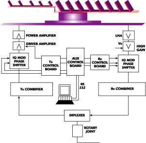
In order to adjust amplitude and phase characteristics of particular sub-arrays, the following method was used in an anechoic chamber. A block diagram of the calibration system is shown in Figure 12.
In the antenna array, the first sub-array without phase shifters is used as a reference sub-array. The antenna is positioned at the minimum angle according to the reference source. At the beginning, the high gain amplifier╒s gates are biased near pinch-off (only the reference sub-array is switched on). The transfer characteristic between the reference source and the reference sub-array (including all amplifiers and power dividers in chain) are measured. The measured amplitude and phase are recorded. After that, a high negative voltage is applied to the reference sub-array (sub-array is switched off) and the first sub-array is switched on (low negative voltage on the high gain amplifier). The phase shift at this sub-array is adjusted by commands from the PC. The phase characteristic is adjusted to be equal to the phase of the reference sub-array.
|
The amplitude characteristic is adjusted by adjusting the gain of the high gain amplifier by setting the appropriate gate voltage. These values are recorded and the sub-array is switched off. This procedure is applied to all sub-arrays. When the last sub-array is measured, all sub-arrays are switched on with the recorded voltages on the I, Q and gate ports. Theoretically, only I and Q signals are enough to compensate the amplitude and phase imbalance, but using the gain control ports gives one more degree of freedom. Practically, the adjusting is much faster because of the small level of AM/PM conversion in the high gain amplifier. The signals received from all sub-arrays with the same phase and amplitude characteristics are added in phase at the output port of the power combiner (that is the beam is positioned in the desired direction). After that, the usual procedure for measuring an antenna is applied.
This procedure is repeated for the antenna positioned at other elevation angles. The values for the entire scanning range can be obtained by interpolation of the control voltages or by measuring in so many steps that beam movement can be discretised.
A similar procedure is applied for the transmitting antenna. The first measurement is made between the first (reference) sub-array and the reference receiver. The phase and amplitude transfer characteristics are recorded. After that, all sub-arrays are switched on sequentially and the phase characteristic is adjusted to approach the same value as the reference sub-array. When all values are recorded, the complete antenna is switched on and the usual measurements of the antenna characteristics are performed. The same procedure is repeated for the different elevation angles.
Measured Results
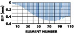
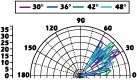
The measurements on the receiving antenna are shown in Figure 13 and agree with the predicted values. The expected suppression of grating lobes of approximately 10 dB below the main lobe was achieved. The overall gain of the receiver is maintained in the range between 39.4 and 40.6 dB. In order to derive properly the gain of the passive antenna arrangement, from the measured value of gain, it is necessary to eliminate the contribution of the chain amplifiers and phase shifters, which in this case is about 10 dB. Assuming an average value of 30 dB gain and a noise contribution of the RF chain of approximately 2.2 dB, and the noise temperature of the clear sky at 45° elevation at 20 GHz, it is possible to evaluate approximately a value of G/T of 5 dB/K.
|

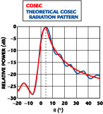
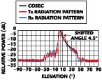
Due to the limitation of the measuring facilities at 30 GHz and current test set-up in the anechoic chamber adapted for measurements of antennas under test on reception, the measurements at Ka-band have been done using a provisional compact range method with a parabolic reflector smaller than recommended. The results of tests in the narrower angular range and with lower accuracy in the phase measurements demonstrate behavior similar to the transmitter antenna measurements. The appearance of higher level of side lobes is due to the impossibility of providing accurate compensation for the phase errors during the process of calibration. The measured radiation patterns of the transmitter are shown in Figure 14.
|
Conclusion
A functional model of a vehicular terminal with scan capabilities has been designed and tested. The low profile contour of the terminal is also achieved. The overall dimensions of the terminal are competitive with the size of its parabolic antenna counterpart. The dimensions of the receiver are 300 x 200 x 80 mm and 240 x 120 x 80 mm for the transmitter. The height of the terminal is 150 mm because the step motor is placed below the rotating platform for the trial. By placing the motor outside of the terminal and transmitting the rotation with belts, it is possible to decrease the height significantly. Also, further integration of the RF chain will have significant impact on the overall dimensions reduction. The proposed antenna configuration is capable of providing an angular beam scan wider than measured (theoretically between 20° and 50° from horizontal).
Acknowledgment
The authors would like to thank Mr. José Alonso, head of the systems division of TTI, for his management and support in the realisation of this project, Dr. José Angel Garcia, University of Cantabria, for his contribution to the design and integration of the LNAs, and Mrs. Laura González, TTI, for her assistance in the antenna design. Also, the authors would like to thank the RF and production division of TTI for its efforts in the fabrication of the terminal, the Alenia-Spazio team, Mr. V. Schena and Mr. G. Losquadro for appreciated support, Dr. Brando Kolundzija from the University of Belgrade, and Dr. Manuel Sierra Peréz and Mr. Pablo Caballero Almena from the Radiation Group of the University of Polytechnic of Madrid for valuable consultations and measurements.
References
- M. Holzbock, A. Jahn, F. Grassl, J. van Noten, M. Pugliese, V. Schena and S. Dragas, "Ka-band Satellite Network Technology: Demonstration of Mobile Services in Multi-segment IP Networks," Proceedings of IST Mobile Communications Summit 2000, Galway, Ireland, October 2000, pp. 663-669.
- V. Schena, G. Losquadro, M. Holzbock, A. Jahn, J. Alonso and S. Dragas, "SUITED Demonstrator Proposal for a New Technology in the Radio Frequency Front-end in the Ka-band Satellite Terminals for Mobile Broadband Applications," Proceedings of IST Mobile Communications Summit 2000, Galway, Ireland, October 2000, pp. 747-752.
- B.M. Kolundzija, T.K. Sarkar, J.S. Ognjanovic and R.F. Harryngton, WIPL(a)V2.0 Electromagnetic Modeling of Composite Wire and Plate Structures, Artech House Inc., Norwood, MA 2000.
- M. Mikavica, Linplan CAD for Linear and Planar Antenna Arrays of Various Radiating Elements, Artech House Inc., Norwood, MA 1992.
- A. Nesic and A. Dragas, "Frequency Scanning Printed Array Antenna," IEEE AP Society International Symposium, Newport Beach, CA, June 1995, pp. 950-953.
- S. Dragas and L. Gonzçlez, "A Simple Solution for the Linear Polarised Antenna for Mobile Terminal," ACES 2002 Conference Proceedings, Monterey, CA, March 2002.
Zoran T. Golubicic received his BSEE degree in electrical engineering from the University of Belgrade, Yugoslavia, in 1982, and joined the Institute of Applied Physics in Belgrade working on projects related with high power RF components. He is currently a research and development engineer at TTI Norte in Santander, Spain. His research interests include nonlinear microwave devices and circuits, and beam pointing systems for phased scan arrays.
Sasa Dragas received his BSEE degree in electrical engineering from the University of Belgrade, Yugoslavia, in 1991, and then joined the Institute of Microwave Technique and Electronics in Belgrade as an R&D engineer, where he worked on passive microwave devices and dual reflector antenna systems. Since 1999 he has worked as an antenna engineer at TTI Norte in Santander, Spain. His present work is focused on the design and investigation of broadband printed antennas and phased scan arrays for the European Space Agency.
Zoran Cvetkovic, after attending Electromechanical College, started his professional career at the Institute of Microwave Technique and Electronics in 1975, working on projects for the development of frequency hopping equipment, high speed synthesisers and digital FM exciter for analogue radio. In 1999, he joined TTI Norte in Santander, Spain, working on PLL synthesiser chips control and adaptive biasing of microwave power amplifiers.