
Traditionally, GaAs based technologies capable of providing solutions at E- and W-Band have been limited to three- and four-inch wafer processing techniques with associated higher running costs. These technologies have generally provided excellent performance but with limited acceptance in moderate volume markets due to associated high MMIC component cost. With the emergence of volume markets in these bands, low-cost GaAs based component solutions are required to meet the cost demands of markets such as E-Band point-to-point communication applications (71 to 76 GHz and 81 to 86 GHz), automotive radar (76 to 77 GHz) and radar systems (93 to 95 GHz).
High frequency point-to-point communication bands at E-Band offer the potential for ultra-high capacity links. The large allocated band offers fiber-like Gbps data rates that far exceed the present performance of the lower frequency microwave radio bands. The ease of installation of the links compared with fiber based solutions point toward this being a long-term solution for high data rate communications in many countries. In the automotive market, autonomous cruise control and emergency braking systems have been developed and successfully deployed on top-end models but until now wider usage has been restricted by the high cost of millimeter-wave components. In these markets and the mainly aerospace focused 94 GHz radar markets, the availability of low cost MMIC based components offers the route to wider market expansion.
Therefore, a key enabling technology for the long-term volume uptake will be the availability of cost-effective semiconductors capable of delivering the required performance at E-Band and above. Recently, GaAs foundries have focused on employing many of the processing techniques and equipment used in the high volume applications of mobile terminals to provide low-cost solutions targeted at these higher frequencies. This has resulted in the release of high performance GaAs based technologies capable of delivering significant gain and power up to W-Band. High performance GaAs based solutions on six-inch wafer technology have the potential to yield low-cost products in the frequency range from 60 to 100 GHz. The enhanced performance of GaAs based solutions, particularly in terms of power and linearity, together with lower development costs makes this the technology of choice on which to develop key functions for volume E- and W-Band applications.
This article describes the design and manufacture of a set of E- and W-Band MMIC power amplifiers based on six-inch 0.1 μm GaAs technology. An overview of the circuit architectures for 22 dBm output power amplifier designs is provided. Measured results of manufactured MMICs show good agreement with simulated results thus demonstrating GaAs MMIC capability to meet the requirements for high performance, low cost E- and W-Band applications.
E- and W-Band MMIC Amplifier Design
The aim of the design process was to realize amplifiers at a range of power levels in the commercial E-Band communication band at 81 to 86 GHz and in the radar band in the 93 to 95 GHz range. Successful demonstration of frequency and power in these bands can be easily translated to the less challenging design at the lower frequency applications in the 60 to 76 GHz range.
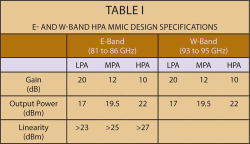
The design philosophy was based on realizing low power amplifiers (LPA), medium power amplifiers (MPA) and high power amplifiers (HPA) in each of the bands. The target specification for each of the amplifiers is shown in Table 1. The LPA can be configured as a local oscillator (LOA), low-noise amplifier (LNA) or as a driver amplifier in the transmit or receive chain. The aim of the HPA specification is to meet the requirements for the output stage of the transmit section for an E-Band radio or as a single MMIC in a multi-MMIC combined HPA for radar applications. In the three design cases, similar circuit features, design approaches and simulation techniques were employed.
The set of E- and W-Band amplifiers were designed on WIN Semiconductor’s PP10 technology which is a 0.1 mm GaAs PHEMT process manufactured on 150 mm wafers. PP10 has an Ft > 135 GHz and Fmax > 185 GHz and is capable of 4 V operation.1 Measured data of the PP10 PHEMT devices was used to ascertain the optimum periphery in terms of power and gain to meet the requirements for each of the amplifiers. Small-signal S-parameter data was supplied by the foundry for a range of different devices sizes (unit gate width and number of fingers). Also, loadpull data was available for a 2×50 μm sized device measured at 30 GHz.2 A GMAX of greater than 10 dB is available for 2×25 and 2×50 μm sized devices. In circuit, this level of gain will not be achieved due to interstage and output network losses, matching for optimum power rather than gain and the influence of any lossy stabilization networks. Published loadpull data indicates that a saturated power density of approximately 0.8 W/mm from a 4 V supply can be achieved. Higher frequency power density data was not available during the design process which offered a level of risk in extrapolating the power density to E- and W-Band. However, the level of gain and low frequency power density indicated that the technology was capable of realizing good amplifier performance in the E- and W-Band.
The LPA was realized as a three-stage design based on 2×50 μm cells for each stage. Although the 2×25 μm cell offered the potential for higher gain, the 2×50 μm cell offered adequate gain coupled with the potential for meeting the power requirements. The four fingered cell approach (4×25 μm) indicated a lower available gain, which may be due to phasing issues across the device due to the narrow input and output feeds for available devices. A common 50 Ω matched structure was used for each stage. This allowed for the potential to easily convert to more stages, or to employ the common cell in multi-function MMICs with other circuit types. The matching networks at the input and output of the 2×50 mm device consisted of a short transmission line and an open circuit stub. Bias was applied to the gate and drain of the PHEMT cells through a bias network consisting of a resonant radial stub and a one quarter wavelength high impedance line. On the power supply side of the radial stub, further lossy decoupling networks were employed to provide a non-reactive termination at low frequencies to ensure oscillation free operation. MIM capacitors were employed to provide DC blocks in the input, interstage and output networks. Further stabilization networks were employed in the input and interstage networks through a parallel R-C network. The intention of this structure was to reduce the lower frequency gain while having a negligible impact on the in-band performance.
A critical aspect of the design is to understand sensitivity of the circuit and to find the best solution for simulation. Previous experience with HPA and amplifier design at lower frequencies pointed toward an approach based on intensive EM simulation of all passive elements; AWR Axiem was employed for the EM simulations. The procedure involves EM simulating entire matching structures and understanding the influence of the active devices on the passive circuit performance. Some level of discrepancy between schematic based and initial EM simulated behavior was present. The circuit was re-tuned until the EM based modeled performance met the electrical requirements.
A similar process was employed for the design of the MPAs. The MPA consisted of two stages of gain. In this case, the output periphery was realized as 2×2×50 μm cells. The two cells were directly combined together in a corporate matched configuration. Although an in-circuit gain of greater than 6 dB is present, the same size driver periphery as the output periphery was employed. This was to ensure that the driver stage had a negligible impact on the power saturation and linearity of the MMIC over the full temperature range and expected process spread. The downside of employing the larger driver is an increase in the DC power consumption and thus a reduction in the total efficiency. Similar circuit features were employed in the MPA as the LPA, in order to apply bias, stabilize the circuit and extract maximum power. Further stability analysis was employed in the MPA to ensure the absence of ‘odd-mode’ and loop oscillation.3,4
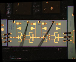
Figure 1 Assembled carrier for E-Band HPA device measurements.
The HPA designs employed 4×2×50 μm cells in the output stage in order to realize greater than 22 dBm of output power. A two stage design was used in order to meet the gain requirements as presented in Table 1. The HPAs were based on two channels of the MPAs which are combined in a corporate approach. This offers a relatively simple and modular approach to increasing the periphery and thus the output power. Further EM simulations were employed in order to ensure that coupling between the two channels was minimal. The symmetry of the HPA is critical, in order to ensure that power is combined in phase.
Measurements
All amplifiers were mounted on a copper tungsten carrier with thermal epoxy. In order to obtain oscillation free operation, external decoupling networks must be applied to the gates and drains of each stage. In a production test environment this can be readily achieved with a custom probe card with integrated decoupling. In this characterization 100 pF single layer ceramic capacitors were bonded to each gate. Further decoupling was applied through bonding universal DC boards consisting of higher value 0402 capacitors onto each gate and drain. Bias was applied to the amplifiers through connecting DC probes to the DC boards. The amplifiers were all directly RF probed and characterized from 75 to 110 GHz. Figure 1 shows a typical configuration for characterization showing a photograph of the E-Band MMIC line-up with associated decoupling networks.
Small-signal measurements were carried out at the Technical University of Graz in Austria. The set uses a ZVA-67 with frequency extensions up to 110 GHz. A set of large-signal measurements were carried out at Filtronic Broadband Ltd. in order to ascertain the power saturation and linearity characteristics of the 81 to 86 GHz amplifier sets. In order to provide sufficient source power, the LPA and MPAs were used as driver devices to provide high gain chains for the HPAs.
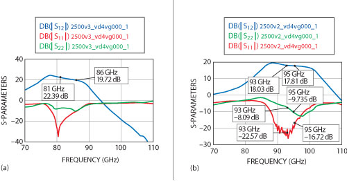
Figure 2 Measured small-signal performance of E-Band LPA (a) and W-Band LPA (b).
Figure 2a shows the small-signal measured performance of the 81 to 86 GHz LPA. Approximately 20 to 22 dB of gain is achieved across the band with an output return loss of better than 11 dB and an input return loss of greater than 8 dB. Figure 2b shows the measured performance of the W-Band LPA that is designed to operate in the 93 to 95 GHz band. Approximately 18 dB of gain is achieved with an input return loss of better than 10 dB and an output return loss of greater than 10 dB. Levels of gain and return losses are close to the simulated performance for both MMICs. Figure 3a shows a measured power sweep for the E-Band LPA at 83 GHz. The saturated power is greater than 17 dBm at the center of the band. This indicates an ‘in-circuit’ power density of approximately 0.6 W/mm that is similar to the expected performance based on the lower frequency extrapolated loadpull data. The best P1dB was achieved when biasing the LPA in a Class AB mode that is at an operating condition away from the peak gain bias point. Figure 3b shows the measured OIP3 as a function of swept power. The best performance was achieved with a bias point of VDS=4 V and VGS=-0.5 V for each stage. A peak output OIP3 of 24 dBm was achieved at a total output power of +10 dBm.
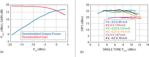
Figure 3 Measured power sweep for E-Band LPA at 83 GHz (a) and OIP3 at 84 GHz (b).
Figure 4a shows the small-signal measured performance of the 81 to 86 GHz MPA. The design is based on a two-stage configuration and exhibits a measured small-signal gain of 12 dB with return losses of better than 10 dB across the band. Figure 4b shows the measured performance of the corresponding W-Band MPA with 11 dB of small-signal gain and return losses of greater than 10 dB across the required frequency band. The E-Band MPA was measured under large-signal conditions and a saturated power of greater than 19.5 dBm was achieved. This is typically in-line with the power density measured for the E-Band LPA previously.
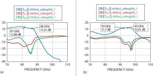
Figure 4 Measured small-signal performance of E-Band MPA (a) and W-Band MPA (b).
Figure 5a shows the measured small-signal performance of the E-Band HPA. A measured gain of greater than 10 dB and with return losses of greater than 10 dB was achieved. Figure 5b shows the measured small-signal performance of the W-Band HPA; greater than 10 dB of gain was achieved with good return losses across the required frequency range. As mentioned previously, in order to measure the power and linearity characteristics of the HPA, the LPA and MPA were employed as driver stages. The devices were connected together through low-inductance chip to chip tape bonds. Figure 6a shows the power sweep for this configuration, biased in a Class AB mode for the center of the frequency band. A saturated power of greater than 22 dBm is achieved in the center of the band, with a P1dB of 21 dBm. This level of saturated power density is similar to that achieved for the LPA and MPA. A slight degradation of the in-circuit power density would be expected due to the extra output combining losses. The OIP3 of the line-up of gain stages is shown in Figure 6b. The measured OIP3 is between 29 to 30 dB for total powers up to +17 dBm. As the output power reaches close to the onset of power saturation, a roll-off in OIP3 is evident. The total gain of the amplifier chain in this configuration is approximately 30 dB.
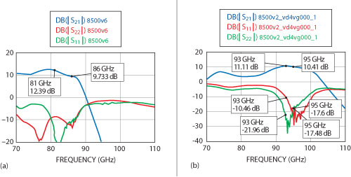
Figure 5 Measured small-signal performance of E-Band HPA (a) and W-Band HPA (b).
Conclusion
E- and W-Band power amplifier MMICs have been designed on six-inch 0.1 μm GaAs technology. Measured results of the manufactured MMICs demonstrated good agreement with simulated results: low power amplifier devices achieved good levels of gain in excess of 20 dB for both E- and W-Band devices. The HPA devices achieved saturated output powers in excess of 22 dBm; tuning of the matching environment will provide further optimized performance. Furthermore, the circuit architecture employed can be easily extended to provide higher levels of output powers. The results presented here demonstrate GaAs MMIC capability is available today to meet the next generation requirements of high performance, low cost E- and W-Band applications.
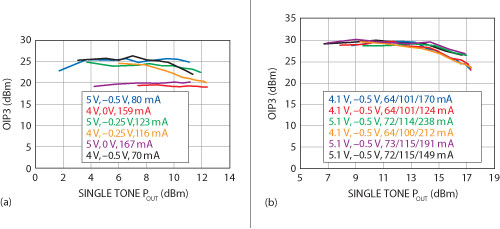
Figure 6 Measured power sweep for E-Band HPA at 83 GHz (a) and OIP3 at 82 GHz (b).
Acknowledgments
We would like to thank the Technical University of Graz (www.ihf.tugraz.at) and Filtronic Broadband (www.filtronic.co.uk) for assistance with measurements.
References
1. WIN Semiconductors Corp., “0.1 mm pHEMT Process for E-band Power Applications,” Microwave Journal, Vol. 53, No. 12, December 2010, pp. 36-38.
2. WIN Semiconductors PP10 Process Design Kit.
3. M. Jankowski, E. Limiti and P.E. Longhi, “Freitag Method Application to PA Stability Test,” IEEE Workshop Integrated Nonlinear Microwave and Millimetre-Wave Circuits, 2008, INMMIC 2008, Issue 24-25, November 2008, pp. 149-152.
4. M. Ohmoto, IEEE Transactions Microwave Theory & Techniques, Vol. 41, No. 6/7, June/July 1993, pp. 983-988.