A Doherty power amplifier using a tunable offset line is proposed for linearity improvement. The conventional offset line is substituted with coupled lines and composite right/left-handed transmission lines (CRLH), incorporating a variable capacitance diode to adjust the phase at the output of the main amplifier, so the phase distortion of the peak amplifier at a high power level can be corrected by tuning the voltage of a variable capacitance diode in the proposed offset line. The performance of the proposed DPA is studied, using numerical simulations, in the frequency range from 2 to 2.5 GHz. The analysis indicates that the proposed DPA, with a tunable offset line, can show an improved linearity at a high input power. The measured results show an excellent IMD3, which agrees with the simulated results. Furthermore, compared to a conventional Doherty PA, the PAE of the proposed amplifier is improved by 5 to 7 percent, while the IMD3 is reduced by approximately 25 dB.
Modern wireless communication systems, such as CDMA and W-CDMA, have critical system requirements for high linearity. Therefore, many power amplifiers are operated to deliver a significantly backed-off average output power. These methods result in low efficiency, due to the over 10 dB back-off. It is difficult to obtain optimum efficiency and high linearity performance in the same Doherty amplifier. The main linearity deterioration of Doherty amplifier occurs in the peaking amplifier, due to the peaking amplifier operating in Class C, which generates high order intermodulation distortion (IMD) products. Many traditional linearization techniques, such as pre-distortion and feed-forward, could be adopted, but these methods require the use of external control circuits and signal processing, resulting in an increased level of design complexity and its linear performance improvement is still limited. In addition, an N-way Doherty amplifier has also been reported for high efficiency and linearity; however, its size and performances have limitations for W-CDMA base station applications.
Composite right/left-handed transmission lines (CRLH) and capacitor-loaded coupled lines can suppress the second and higher order harmonics of the output1,2,3 and at the same time, the structure exhibits either a negative or a positive phase, as well as a 0 phase, according to the design needs.4 Due to its compact and flexible design, the structure lends itself easily to integration with other microwave components and devices. Recently, some works were reported to improve the linearity of Doherty amplifiers by composite right/left-handed transmission lines and defected ground structure (DGS).5,6 Because harmonic components play a positive role in improving PAE and linearity, the CRLH and DGS are used to suppress second and other order harmonics of the main amplifier output. However, at a high power level, the phase distortion of the peaking amplifier still cannot be solved, so the linear improvement is also limited. The inherent linearity deterioration of a Doherty amplifier sets a threshold for achievable performance.
In this article, tunable CRLH and coupled lines, using a variable capacitance diode in an offset line to improve linearity performance of a Doherty amplifier, is introduced. The tuning voltage of a variable capacitance diode,7 the tunable CRLH and coupled lines, can be adjusted to adopt any phase and this makes the design more flexible and usable. The proposed structure is shorter by 7 to 12 mm in length than the offset line of a conventional one. The proposed structure suppresses the second and higher order harmonics of the main amplifier output and, at the same time, the phase distortion of the peaking amplifier at a high power level can be corrected by tuning the voltage of a variable capacitance diode in CRLH and coupled lines. The proposed tunable offset line method not only fulfills the phase delay and phase correction, but also results in some other improvements, such as higher PAE and improved linearity.
Fundamental Theory
Circuit Description
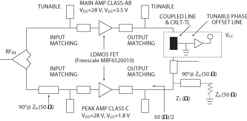
Figure 1 Proposed architecture of a DPA using a tunable offset line.
In the proposed tunable Doherty amplifier, the conventional offset line is replaced with a variable capacitance diode loaded CRLH and coupled lines to suppress the harmonics and adjust the phase with the variable capacitance diode. The proposed structure makes the design more flexible and makes many other improvements in the Doherty amplifier. The topology of the circuit is shown in Figure 1. The main amplifier (Class AB) signal, passing through a tunable offset line and a λ/4 transmission line, is combined with the peak power amplifier (Class C) signal at the output. Due to the Class AB of the main amplifier, the linearity of the entire Doherty amplifier is ensured and, at the same time, with the peak amplifier operating in Class C, the efficiency of the entire Doherty amplifier also is improved. The tunable offset line consists of variable capacitance diode-loaded coupled lines or variable capacitance diode-loaded CRLH. The Ropt and Z0 are used for the load impedances of the main and peak amplifiers, respectively. The Ropt is selected as 2Z0 for matching and decreasing power leakage to the peak amplifier when the peak amplifier is turned off, and when it is turned on, Z0 is 50 Ω and Z1 is

Figure 2 shows a tunable offset line using variable capacitance diode-loaded coupled lines. The structure consists of a variable capacitance diode load and a pair of the symmetrical parallel coupled-lines. The harmonic suppression and variable phase are achieved by the variable capacitance diode loaded coupled lines. The impedance of the tunable offset line is 50 Ω, and the phase of the offset line can be modified through changing the voltage of the variable capacitance diode. The modifying phase of the main power amplifier will be more flexible, so that the phase distortion of the peaking amplifier at high-power level will be cancelled. Therefore, the performance of the proposed Doherty power amplifier (DPA) can be improved much more than with a DPA using a conventional offset line. The other tunable offset line is a variable capacitance diode loaded CRLH. The variable capacitance diode-loaded CRLH replaces the conventional offset line, where the right-handed transmission line (RHTL) and the left-handed transmission line (LHTL), are composed of capacitors and inductors. When the series and shunt resonances are equal, the structure is said to be balanced. According to the desired phases for two different frequencies, the phase response of CRLH-TL will be -π/2 at f1 (fundamental frequency) and -2π f2 (second harmonic). Therefore, a large portion of the second harmonics generated from the main and peaking amplifiers will be cancelled at the summing load. Furthermore, at high-power level, the phase distortion of the peaking amplifier will be corrected through the tuning voltage of the variable capacitance diode.

Figure 2 Proposed offset line using a variable capacitance diode-loaded coupled lines (a) and using variable capacitance diode-loaded CRLH.
Linearity Analysis
At low-power level, the IMD3 of the entire DPA is only provided by the main amplifier, while the peak amplifier is turned off, due to the suppression of harmonics at the output of the main amplifier in the proposed DPA. Compared to the conventional offset line structure, the second and higher order harmonics of the main amplifier are effectively suppressed from 3.5 to 7 GHz by the proposed structure. The AM-AM distortions of the proposed DPA are lower than that of a conventional DPA.
At high-power level, while the peak amplifier is turned on, IMD3 is a composite of contributions from both the main and peak amplifiers, the output phase distortion of the Doherty amplifier comes mainly from the peak amplifier, while the carrier amplifier is biased at Class AB operation. In this case, the nonlinear output current of the active devices can be approximately expressed by a Taylor series expansion:

where vi is an input voltage and gmx is the xth-order expansion coefficients of the nonlinear transconductance. The third-order intermodulation distortion (IMD3) current is mainly generated by the gm3vi3 term of Equation 1. Assuming that the load modulation does not seriously affect linearity and that the main amplifier is biased as Class AB to have a gm3 of -a, the bias of the peaking amplifier for the two-way Doherty amplifier should be adjusted to have a gm3 of a to perfectly cancel the IMD3 current generated by the main amplifier. However, the bias point of the peaking amplifier for a perfect IMD3 cancellation may approach closely to a Class B bias. Furthermore, a Class C biased peak amplifier brings a lot of AM-AM and AM-PM distortion at high power. The AM-AM and AM-PM distortions of the peak amplifier can result in IMD3 deterioration. However, in the proposed DPA, the phase distortion of the peak amplifier can be corrected by tuning the phase of the main amplifier, so that the phase distortion and gm3 of the proposed entire DPA can be decreased. Therefore, the IMD3 of the entire DPA is improved. In the proposed DPA, tuning the variable capacitance diode-loaded coupled lines or the variable capacitance diode-loaded CRLH at the output of the main amplifier can correct the phase distortion of the peak amplifier. At the same time, the second and higher order harmonics of the main amplifier output are largely suppressed, so the linearity of the proposed DPA is improved.
Realization of the Linear Amplifier based on a Tunable Offset Line
Tunable Varactor Diode-loaded Coupled Lines for Offset Line
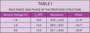
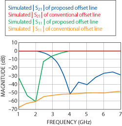
Figure 3 Simulated S-parameters of the varactor diode-loaded coupled lines and conventional offset line.
The schematic diagram of a tunable offset line, using varactor diode-loaded coupled lines, was shown previously. The tunable offset line consists of a variable capacitance diode load and a pair of symmetrical parallel coupled-lines with a length Lc, a width W and a slot S between the lines. The phase of the offset line varies according to changes in capacitance of the diode, which are obtained by tuning the reversed voltage of the diode. The reactance and variable phase of the proposed structure are shown in Table 1 for the frequency range from 2010 to 2100 MHz, where, Lc, S and W are 4, 0.2 and 0.5 mm, respectively. Cs is the equivalent value of the varactor diode. In addition, a 50 Ω tunable offset line is chosen to match the λ/4 transmission line. The simulated S-parameters of the varactor diode-loaded coupled lines and the conventional offset line are shown in Figure 3, compared to a conventional offset line. The second and higher order harmonics in the varactor diode-loaded coupled lines is largely suppressed. The rejection band is extended from 3.5 to 7 GHz with a rejection ratio more than 20 dB. In the total process of DPA operation (low and high power level), the linearity of the main amplifier, and also of the overall Doherty amplifier improved, due to the suppression of the second and higher harmonics at the main amplifier output in the proposed structure. The optimized performances are shown on the basis of a 23.2° offset line.
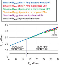
Figure 4 Simulated AM-AM distortions in DPA using a tunable coupled line and a conventional DPA.
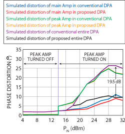
Figure 5 Simulated AM-PM distortion in DPA using a tunable coupled line and a conventional DPA.
Figures 4 and 5 show the simulated AM-AM and AM-PM distortions of the proposed and conventional DPAs. At low-power level, the IMD3 of the entire DPA is only provided by the main amplifier, while the peak amplifier is turned off. The phase distortion in the conventional DPA is almost the same as that of the proposed DPA. Due to the suppression of harmonics in the output of the main amplifier in the proposed DPA, the AM-AM distortions in the proposed DPA is lower than that of a conventional DPA. At high-power level, while the peak amplifier is turned on, IMD3 is a composite of the contributions from both the main amplifier and peak amplifier. The harmonics of the main amplifier are suppressed by the proposed coupled line. While Pin is 30 dBm, the Pout distortion of the proposed DPA is improved by as much as 3.6 dB over that of the conventional DPA. Furthermore, at high-power level, the phase distortion of the peak amplifier (Class C) is large, which will result in the deterioration of IMD3. However, the gm3 parameters of the FETs are opposite in the peak and main amplifiers of the proposed DPA. The phase distortion of the peak amplifier can be corrected by tuning the phase of main amplifier, so that the phase distortion and gm3 of the proposed entire DPA can be decreased. Therefore, the IMD3 of the entire DPA is improved. In the proposed DPA, tuning the reversed voltage of the varactor diode-loaded coupled lines at the output of the main amplifier can correct the phase distortion of the peak amplifier. As shown, the simulated AM-PM distortion is improved in the proposed DPA, especially, when Pin is 30 dBm, the phase distortion of the proposed DPA is improved by 19.5° over that of a conventional DPA.
Tunable Varactor Diode-loaded CRLH for Offset Line
To achieve the tunable offset line, a variable capacitance diode-loaded CRLH can also be adopted. The configuration of the proposed offset line was shown previously. The proposed structure is composed of a varactor diode and CRLH. The CRLH is realized by loading a conventional transmission line (TL) with lumped element series capacitors (C) and shunt inductor (L) where the length and width of the right-handed transmission line in CRLH are lm and wm, respectively. When the series and shunt resonances are equal, the structure is said to be balanced, ZOR, ZOL and ZoCRLH are fixed as Zoffset. The characteristic impedance of the tunable offset line and the λ/4 transmission line can be obtained by a load modulation technique. The CRLH can be designed using P and Q, where P and Q are
 And
And 
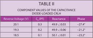
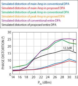
Figure 6 Simulated AM-PM distortion in DPA using tunable CRLH and a conventional DPA.
respectively.The RH TL has a negative phase response (phase lag) proportional to, whereas the LH TL has a positive phase response (phase lead) proportional to .P, Q, ZOR and ZOL are altogether used to determine C, L and the physical length of RH-TL. When C and L are 10 pF and 42 nH, and lm and wm are 4 mm and 1 mm, respectively, the reactance and variable phase of the proposed structure is shown in Table 2, in the frequency range from 2010 to 2100 MHz. Because the second harmonics generated in the main and peaking amplifiers will be cancelled at the summing load, while the peak amplifier is turned off, harmonics cannot be suppressed, so the linearity is not improved. At high-power level, the peak amplifier is turned on when the main amplifier reaches saturation, tuning the reversed voltage of varactor diodes in CRLH, the phase distortion of the peak amplifier at high-power level can be corrected. As shown in Figure 6, at high-power level, compared to a conventional Doherty PA, the simulated AM-PM distortion of the proposed Doherty PA is reduced by 12.3 dB (Pin is 31 dBm).
Simulated and Measured Results
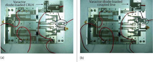
Figure 7 Photographs of DPAs using a varactor diode-loaded CRLH (and coupled lines (b).
The proposed Doherty power amplifier was simulated using Agilent ADS from 2 to 2.5 GHz. Figure 7 shows the photographs of the fabricated proposed Doherty amplifiers (varactor diode-loaded CRLH and varactor diode-loaded coupled line), where a Taconic RF35 substrate (εr =3.5 tan δ=0.001) was used. The Microsemi’s KV2111 and Philips’s BB181 varactor diodes are chosen for the tunable coupled line and tunable CRLH, respectively. The phase of the offset line is tuned at -21°, -23° and -27° by adjusting the voltage of the varactor diode manually. The optimized PAE and linearity is achieved with a -23° phase offset line. The PAE of the DPA is simulated by using load/source pull and harmonic balance methods. The PAE is measured by calculating Pac/Pdc, where Pac is the difference between Pout and Pin. Pdc is calculated from the voltage and current of the power supply. At high-power level, a better match at the output of the main amplifier is achieved and at the same time, the parameter γ is optimized using the tunable offset line, so the total efficiency of the Doherty amplifier system is improved. The measured and simulated PAEs of the proposed DPA and conventional PDA are shown in Figure 8. At low-power level (Pout under 29 dBm), the peak amplifier is turned off and the PAE of the proposed DPA is the same as that of the conventional DPA. For Pout above 29 dBm, the peak amplifier is turned on and the voltage of varactor diode is adjusted to optimize the match and compensating phase. Consequently, the PAE of the proposed DPA is improved. The measured and simulated PAE of the proposed DPA is greater (5 to 7 percent) than that of the conventional DPA. The maximum measured PAE of the proposed DPA is 45.2 percent at 2.01 GHz.
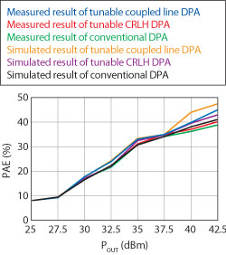
Figure 8 Measured and simulated results (PAE) of the proposed DPA and conventional DPA.
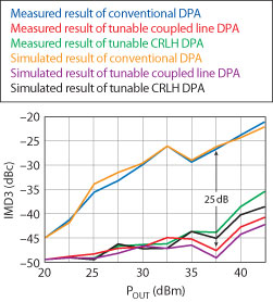
Figure 9 Measured and simulated IMD3 of the proposed DPA and conventional DPA.
Figure 9 shows the measured and simulated IMD3 performance of the proposed DPA using two-tone signals at 2015.5 and 2020.5 MHz (the tone spacing is 5 MHz). In the proposed DPA, the harmonic of the amplifier is suppressed. At the same time, the phase distortion of the peak amplifier and gm3 of the proposed entire DPA can be decreased by tuning the proposed offset line, so the IMD3 of the two proposed DPAs were considerably improved compared to that of the conventional DPA. The IMD3 of the DPA using the tunable CRLH is not as good as that of the DPA using a tunable coupled line, mainly because the harmonic of the DPA cannot be suppressed while the peak amplifier is turned off and the phase of the second harmonic deviates a little from -2 π, while tuning the tunable offset line at high-power level. At low-power level (Pout under 29 dBm), the peak amplifier is turned off and the harmonic of the main amplifier is suppressed by the proposed structure. IMD3 is improved over that of the conventional one. At high-power level (Pout above 29 dBm), the peak amplifier is turned on, the phase of main amplifier and gm3 are modified by tuning the voltage of the varactor diode and the distortion of the peak amplifier output is corrected. The IMD3 is improved by approximately 25 dB better than that of a conventional one. The data shows the improvement in linearity due to lower harmonics and the decrease of the phase distortion and gm3.
Conclusion
A Doherty power amplifier, using a tunable offset line, is proposed to improve linearity and PAE. The tunable offset line is achieved by two structures, one is a varactor diode loaded coupled line, the other is a varactor diode-loaded CRLH. The proposed structure is utilized to suppress second and higher order harmonics and, at the same time, it can correct the phase distortion of the peak amplifier and decrease the gm3 of the entire DPA by tuning the voltage of the varactor diode at high-power level. In addition, tuning the phase in a DPA becomes more flexible with the proposed structure. Testing results show that the linearity of the proposed DPA has been improved by 25 dB over the conventional DPA, which verifies the advantages of the proposed structures.
References
- M.A. Antoniades and G.V. Eleftheriades, “Compact Linear Lead/lag Metamaterial Phase Shifters for Broadband Applications,” IEEE Antennas and Wireless Propagation Letters, Vol. 2, No. 7, July 2003, pp. 103-106.
- S.H. Ji, S.K. Eun, C.S. Cho, J.W. Lee and J. Kim, “Linearity Improved Doherty Power Amplifier Using Composite Right/Left-Handed Transmission Lines,” IEEE Microwaves and Wireless Components Letters, Vol. 18, No. 8, December 2008, pp. 533-535.
- Y.C. Jeong, S.G. Jeong, J.S. Lim and S. Nam, “A New Method to Suppress Harmonics Using l/4 Bias Line Combined by Defected Ground Structure in Power Amplifiers,” IEEE Microwaves and Wireless Components Letters, Vol. 13, No. 12, December 2003, pp. 538-540.
- Y. Yu, Y. Liu, S. Li and S. Li, “A Novel High-power Amplifier Using a Generalized Coupled-line Transformer with Inherent DC-block Function,” Progress in Electromagnetics Research, Vol. 119, 2011. pp. 171-190.
- Y. Yang, J. Yi, Y.Y. Woo and B. Kim, “Optimum Design for Linearity and Efficiency of a Microwave Doherty Amplifier Using a New Load Matching Technique,” Microwave Journal, Vol. 44, No. 12, December 2001, pp. 20-36.
- Y. Zhao, A.G. Metzger, P.J. Zampardi, M. Iwamoto and P.M. Asbeck, “Linearity Improvement of HBT-based Doherty Power Amplifiers Based on a Simple Analytical Model,” IEEE Transactions on Microwave Theory and Techniques, Vol. 54, No. 12, December 2006, pp. 4479-4488.
- I. Lin, M. Devincentis, C. Caloz and T. Itoh, “Arbitrary Dual-band Components Using Composite Right/Left-Handed Transmission Lines,” IEEE Transactions on Microwave Theory and Techniques, Vol. 50, No. 4, April 2004, pp. 1142-1149.
