
A considerable research effort has been invested to optimize the efficiency of high frequency power amplifiers. The work has been focused on output load network design for high frequency active devices. However, the attention received by the driving waveforms and input circuits has been quite low compared to that of the load network. From a system point of view, power-added efficiency, which includes the driving power, is a more important design parameter than the collector or drain efficiency to optimize the overall efficiency.
Therefore, a comprehensive review of high frequency power amplifier driving methods and techniques is crucial to optimize the overall system efficiency. This work is divided in two parts: Part 1 focuses on the use of a low frequency approximation for research on high efficiency power amplifier methods and circuits; Part 2, to be published later, will be devoted to the essential high frequency analysis.
Problem Description
There is little scientific literature about power amplifier driving circuits and most of it is dedicated to low frequency amplifiers or power converters up to some tens of megahertzs.1–4 The operation of low frequency active devices is different than for their high frequency counterparts. The same assertion is valid for their characterization and modeling — ordinary low frequency driving concepts, such as “gate charge,”5 are not specified for high frequency devices. Hence, the design concepts for low frequency amplifiers can hardly be used for RF and microwave circuits.
The main difference between active devices working at high and low frequencies relies on the fact that the inherent capacitances of high frequency devices offer very low reactances. These low reactances determine the device’s behavior in high efficiency RF and microwave amplifiers. While input and output capacitances are not the most important problem (because they can be absorbed by external matching networks), the low reactances associated with the capacitances across the input and output device ports can seriously affect the device’s behavior and its driving requirements.
The most popular RF high efficiency classes (such as class-D and class-E)6 are based on active device switching. These amplification modes require low saturation resistances to achieve high efficiency operation. Thus, large area devices are required to provide low saturation resistance. On the other hand, large area devices exhibit large intrinsic capacitances and the problem related in the previous paragraph gets worse.
This article focuses on the analysis of the driving methods for field-effect, high frequency transistors, because at present, this kind of device is the most usual choice for RF and microwave power applications. The driving methods analysis for bipolar devices will be covered in a future article.
High Frequency Active Device Modeling
Low frequency (up to some tens of megahertzs) switching circuits using MOS devices are usually analyzed and designed using the “gate charge” concept.5 Gate charge measurement specifies the charge required to force the active device to switch under some specific conditions. Most power device manufacturers specify both gate charge and intrinsic capacitance for their products.
However, the gate charge parameter is not used for RF and microwave devices. High frequency MOS manufacturers only provide intrinsic capacitance measurements, large-signal impedances and even nonlinear models for most widely used simulators. These data are not sufficient to design effective driving circuits for high efficiency amplifiers.
The analysis contained in this article is based on a very simplified model for enhancement-mode MOS devices. Two models are proposed, one for low frequency operation and the other for high frequency. The main difference between these models relies on the capacitance CDG across the gate and drain terminals. This capacitance is neglected in the low frequency model because its reactance is considered too low to influence circuit operation. These models are shown in Figure 1.
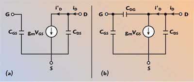 | ||
| Fig. 1 MOS transistor models; (a) low frequency and (b) high frequency. | ||
The main characteristics of these models are:
- The threshold voltage is VTH = 0 V.
- The transistor is modeled in the active (saturation for MOS nomenclature) region by a voltage-controlled current source. The transconductance of this controlled current source gm is considered constant.
- The transistor is modeled as an open circuit for the voltage across the gate-to-source terminals vGS(t) < VTH.
- For the sake of simplicity, all the device intrinsic capacitances are constant and do not depend on the voltage across them.
- Only the semiconductor effects (die) are modeled; the package parasitics and wire bonding effects are considered embedded in the external networks.
Figure 2 shows the current-to-voltage transfer and the output characteristics of the active device used in this analysis.
 | ||
| Fig. 2 MOS output and transfer characteristics. | ||
Driving Analysis Using Class of Amplification Concept
Usually high frequency amplifiers have been analyzed using the amplification class concept. This classification is based on the load conditions, both at fundamental and harmonic frequencies, and on the drain (collector) current conduction angle. The present analysis is also based on the amplification class theory but it is focused on the driving signal and source impedances needed to achieve the desired operation mode rather than the load conditions.
Class-A Amplifier
Class-A amplification has been associated with applications requiring linearity. This statement is usually true, especially when no maximum voltage and current excursions are involved.
Much literature exists, covering small-signal class-A amplifier analysis and design.7 These analysis techniques use small-signal scattering parameters to determine the optimum load and source impedances. For the design of class-A power amplifiers, the Cripps method8 is widely accepted. Both techniques (Cripps method and small-signal analysis) can be used together to design linear class-A amplifiers and to determine the load and input impedances. Using these theories, it is easy to calculate the driving power needed for class-A power amplifiers. If the device is unconditionally stable and can be simultaneously matched at its input and output ports, the driving power can be simply obtained by dividing the power delivered to the load by the maximum available gain of the device (for a small-signal design). No more effort will be dedicated to this topic; the interested reader can review the referenced literature. Nevertheless, some remarks not included in those design techniques will be presented in the next few paragraphs.
It seems logical that the natural driving waveform for the class-A power amplifier is a sinusoidal voltage (for a constant transconductance device). The output waveforms, such as drain current i'D (t) and drain to source voltage vDS(t), are also sinusoidal. The required load impedance is purely resistive at the fundamental frequency and the load presented at the harmonics does not matter.
However, in a real case, sinusoidal waveforms only exists for small excursions of the input and output waveforms. The transconductance gM can hardly be considered to be constant for large output current and voltage excursions. Neither the input gate capacitance, CGS, or the output capacitance, CDS, can be considered constant for large voltage variations. Thus, if a class-A power amplifier is driven by a voltage source with low internal source impedance, a perfect sinusoidal gate current IG(t) should not be expected.
Class-A Amplifier Analysis: Low Frequency Approximation
The driving power required by a class-A power amplifier is calculated for the maximum output current i'D(t) and voltage vDS(t) excursions using the low frequency model shown. The analysis conditions are:
- CGD is neglected (low frequency approximation).
- The driving voltage is able to produce maximum output excursion but no saturation is allowed.
- The maximum peak output voltage VOM is equal to the supply voltage — VOM = VDC.
- The MOS output capacitance, CDS, is resonated at the operating frequency using the load ZL. Thus, the voltage-controlled current source of the model “sees” a pure resistive load at the operating frequency. This fact also means that the output current i'D(t) is in perfect phase opposition with the drain-to-source voltage vDS(t).
- The value of the resistive load is obtained using the Cripps method for maximum output power.8 Figure 3 shows the schematic of the class-A amplifier under analysis.
 | ||
| Fig. 3 Class-A amplifier circuit schematic. | ||
To analyze this circuit, simultaneous maximum output current i'D(t) and voltage excursions vDS(t) are required. However, to keep the device working in class-A conditions, saturation is not allowed. Figure 4 shows the vDS(t) and i'D(t) waveforms and the gate-to-source voltage vGS(t) needed to achieve those output waveforms.
 | ||
| Fig. 4 Class-A input and output waveforms. | ||
The drain current i'D(t) is related to the input gate-to-source voltage vGS(t) through the constant transconductance gm. In this way, the following few remarkable voltage levels at the MOSFET gate can be established:
- V'BIAS is the bias gate-to-source voltage required to achieve the drain bias current IBIAS at the output.
- V'SAT is the maximum gate-to-source voltage allowed at the input of the active device. The V'SAT voltage drives the active device to the boundaries of saturation.
From the waveforms shown, the peak gate current IG for maximum output excursion can be derived as

The driving power PG can be calculated as

When using an input series resonant circuit, the source voltage required is

It is obvious that if no input resonant circuit is used (L = 0) the driving power PG is the same, but the source voltage must be increased. This means larger power losses.

It is important to analyze the charge acquired by the input capacitance CGS and the time employed to acquire it. Figure 5 shows the voltage across CGS.
 | ||
| Fig. 5 Class-A Vgs (t) voltage across Cgs. | ||
The maximum charge acquired by CGS is QCgs = CGSVSAT (coulombs). It is important to note that this charge must be supplied to the gate in a half period of the driving signal (π radians).
Classes AB, B and C Analysis: Low Frequency Approximation
The most important reduced angle amplification classes (AB, B and C) are based on the following principles: the active devices operate in the cut off and active regions, saturation is not allowed, a resistive load impedance is required at the fundamental frequency, short-circuits at the harmonics, and the drain current conduction angle is less than 360°. The driving voltage waveform, for class-B power amplifier operation, vGS(t), is shown in Figure 6.
 | ||
| Fig. 6 Class-B Vgs(t) waveform. | ||
The usual way to generate the driving waveform required for a class-B amplifier is to employ a sinusoidal voltage driving waveform combined with the nonlinear transfer characteristics of an active device (conduction for vGS(t) > VTH, cut off for vGS(t) < VTH). Thus, CGS must be charged from VTH up to the gate-to-source voltage vGS(t) = V'SAT. The charge acquired in this process is QCgs = CGSV'SAT coulombs. Afterwards, CGS is discharged down to VTH. The energy used in the charging process is E = 1/2CGS(V'SAT)2 joules. It is important to realize that the angular time required for the charging and discharging process is the same — π/2 radians (half of the time used for charging CGS in class-A operation).
However, because of the sinusoidal shape of the driving voltage, the capacitance CGS must be charged with reverse voltage from VTH up to –VSAT and again discharged down to VTH during the cut-off period. The energy supplied during this process is also E = 1/2CGS(V'SAT)2 joules. Obviously the energy used to charge CGS during the cut-off period is wasted. This energy is not converted into energy at the output of the device (no resonant input circuit is considered).
It is clear that the conventional driving method for reduced angle classes is simple but exhibits important energetic disadvantages that are directly translated into gain reductions. When driving a class-B amplifier in the usual way, a 6 dB gain reduction may be expected compared to a class-A amplifier using the same device, delivering the same output power and operating at the same supply voltage and frequency (constant transconductance is assumed).
The practical advantages of the conventional driving method are the existence of sinusoidal gate-to-source voltage vGS(t) and current Ig(t). The process is completely linear (at least for this simplified model) and a series resonant circuit at the input can be used.
In order to make the best use of the driving energy, the driver should generate only a half sinusoidal gate-to-source voltage vGS during the conduction period and a constant voltage equal to VTH during the cut-off period. The most evident way to generate this driving voltage from a sinusoidal waveform is by using a nonlinear circuit. This circuit also has to take into account the source impedance, not only at the fundamental, but also at the harmonics, to allow the required gate current IG(t) to flow. These current and voltage waveforms are the dual of those found at the output of the device in class-B operation:
Class-B output conditions:
- Output voltage vDS(t): sinusoidal.
- Output current i'D(t): half sinusoidal.
- Output circuit: parallel resonance (short circuits at the harmonics).
Class-B proposed input conditions:
- Input voltage vGS(t): half sinusoidal.
- Input current IG(t): sinusoidal
- Input circuit: serial resonance (open circuits at the harmonics).
High Efficiency Classes Analysis: Low Frequency Approximation
There are several techniques and topologies used to design low frequency drivers (up to some tens of megahertzs) for high efficiency power amplifiers. Scientific literature and application notes exist, and even some integrated circuits are marketed.2,3 Nevertheless, there is little mentioned about driving circuits and techniques for power amplifiers at high frequencies.
Classes D, E and F are the most popular amplification modes for high efficiency operation at high frequencies. Among them, classes E and F are the most suitable for RF and microwave operation. Class-E6 is known for its high efficiency and its inherent capabilities to work in high frequency circuits (using intrinsic devices capacitances and package parasitic embedded into load networks). Class-E is based on switching active devices instead of controlled current sources. Any efficient driving method for class-E amplifiers must minimize the energy used to force the devices to switch.
The following sections analyze the most popular driving methods used with high efficiency class-E amplifiers. An analysis considering high frequency conditions will be presented in Part 2.
Low Source Impedance Square Voltage Source Driving: Low Frequency Approximation
Square voltage driving at high frequencies is quite difficult to implement. Most popular drivers based on this principle, like the “totem-pole” driver, use two complementary transistors (NPN and PNP bipolars or N and P channel MOSFETs) and cannot work at RF and microwave frequencies.
Assuming the transistor model shown previously, the energy required to charge the input capacitance CGS from the threshold voltage VTH (VTH = 0 for this model) up to the minimum input voltage for device switching VSW is

This energy must be supplied twice every period, the first time to charge the capacitance CGS and the second time to discharge it. The driving power required for these charging and discharging operations is
![]()
VSW is the minimum gate-to-source voltage that makes the transistor switch (at RF frequencies, switching is tantamount to saying that the drain-to-source impedance is low). This voltage depends on the device transfer characteristics and the output load. Usually VSW is greater than V'SAT (V'SAT is the gate-to-source voltage required to saturate the device in class-A conditions) for the same power, voltage and frequency conditions.
 | |||
The driving power, PGSQ, is independent from the internal voltage source resistance R.9 Nevertheless, the time required to charge and discharge the capacitance, CGS, and the maximum gate current, IG, do depend on this resistance R. Time is the most important factor to determine the switching time of a MOS transistor. Thus, the charging and discharging time of CGS should be as short as possible because the efficiency of the amplifier strongly depends on it.
From early class-E literature, it is known that the main switching losses associated with this amplification class (something similar happens with other classes) happen during the on-to-off switching instants10 (drain to source voltage vDS(t) and drain current i'D(t) are very low during the off-to-on switching instants). Kazimierczuk11 related the drain current fall time with the drain efficiency ![]() D, as shown in Table 1, where T = 1/f is the input signal period.
D, as shown in Table 1, where T = 1/f is the input signal period.
In order to keep a high drain efficiency, the charging and discharging time of the input capacitance CGS must be kept inside these boundary limits. To illustrate this process, Figure 7 shows the voltage waveforms vGS(t) obtained with a square voltage driving signal for an ideal condition (R=0) and a real one (R≠0). R is the internal source resistance of the square voltage source. The gate current IG(t) is also shown.
 | ||
| Fig. 7 Vgs(t) and Ig(t) for square wave driving. | ||
For the real case, the most interesting one for this analysis, the discharging time of CGS can be considered equal to the fall time tf. From basic circuit theory, the equations for the gate-to-source voltage VGS(t) and the gate current iG(t) during the discharging can be derived as

 | |||
After three time constants 3![]() the voltage across CGS is vGS=0.05VSW and the transistor can be considered in cut-off mode. Table 2 relates the maximum value of the time constant
the voltage across CGS is vGS=0.05VSW and the transistor can be considered in cut-off mode. Table 2 relates the maximum value of the time constant ![]() with the maximum drain efficiency
with the maximum drain efficiency ![]() D. These results have been derived relating the discharging time with the Kazimierczuk results shown in Table 1.
D. These results have been derived relating the discharging time with the Kazimierczuk results shown in Table 1.
The following example uses the results displayed in Table 2 to calculate the driving power and source resistance required for a commercial Motorola LDMOS driving circuit. The MRF183 (45 W at 28 V, 945 MHz) exhibits an input capacitance CISS = 90 pF (published by the manufacturer). To drive this LDMOS at 100 MHz with a square voltage, a source resistance lower than 3.3 Ω is required to achieve a 95 percent drain efficiency, and a source resistance lower than 6.6 Ω for an efficiency better than 90 percent.
A new parameter, the minimum switching driving power PGmin, will be defined for better understanding. This is the minimum power needed to force a device embedded in a high efficiency power amplifier to switch. PGmin is calculated from

where
VSWmin = minimum gate-to-source voltage excursion required for device switching
For example, assuming a minimum switching voltage VSWmin = 5 V, the minimum switching driving power required by the MRF183 working in the previous example amplifier is
PGmin = 90 x 10–12 x 52 x 100 x 106
= 0.25 W
In fact, this is only an approximate calculation. Other factors like gate losses and padding resistor losses (for stabilization purposes) are neglected. In summary, an effective gate driving system requires both a driving power level equal or greater than PGmin and a CGS charging time as short as possible.
Sinusoidal Driving
It was mentioned before that there are serious technological limits to manufacture square wave drivers for high efficiency RF and microwave amplifiers. Therefore, RF and microwave amplifiers are usually driven using sinusoidal voltage waveforms. From Figure 8, it is obvious that driving a high efficiency power amplifier with a sinusoidal voltage exhibiting a peak-to-peak voltage equal to VSW (VPP = VSW) is not possible. The charging time of the input capacitance CGS is larger than the maximum allowed for high efficiency operation. Thus, the peak-to-peak voltage of the sinusoidal driving voltage must be larger than VSW to minimize CGS charging time and subsequently drain current fall time tf.
 | ||
| Fig. 8 Class-E sinusoidal driving waveforms. | ||
The relation between the minimum switching voltage VSW and the peak voltage Vpeak can be calculated using Kazimierczuk results and some trigonometric relations. These results are shown in Table 3.
 | |||
Obviously, the peak-to-peak voltage (VPP = 2Vpeak) must be lower than the maximum gate-to-source voltage rating of the transistor.
The gate current iG(t) is also sinusoidal. The peak value of gate current is
![]()
If the gate circuit is resonant (series resonance) the driving power PG required with a sinusoidal driving can be calculated as
From Equation 10 the required driving power for 90 percent drain efficiency is

For 95 percent drain efficiency

These power levels can be related with the minimum driving power using a square driving voltage PGmin
PG90 = 2π2RCgsfPGmin (13)
PG95 = 4.5π2RCgsfPGmin (14)
Applying these equations to the Motorola MRF183 LDMOS working at 100 MHz and driven by a 100 MHz sinusoidal voltage source (5 Ω internal resistance) the following results are obtained
PG90 = 0.9 PGmin (15)
PG95 = 2 PGmin (16)
The same transistor working at 500 MHz gives
PG90 = 4.5 PGmin (17)
PG95 = 10 PGmin (18)
Nevertheless, some practical issues must be taken into account. The gate internal resistance and other secondary effects have been neglected in these calculations, so the driving powers obtained with Equations 14 and 15 are approximations. It must be remembered that PGmin is the power needed to achieve a theoretical 100 percent drain efficiency, while the calculated driving power levels achieve “only” 90 and 95 percent theoretical drain efficiency.
However, even using this approximation, it is easy to derive the following few consequences:
- The driving power increases with internal source resistance.
- The driving power increases with frequency.
- Sinusoidal driving requires more driving power PG than square wave driving (PGSQ) to achieve similar drain efficiency levels.
Conclusion
An analysis of power amplifier driving methods and circuits based on a simple, yet effective, low frequency active device model has been performed. Important conclusions have been derived about the inherent inefficiency associated with the most usual (because of their simplicity) driving methods used with power amplifiers. Some interesting concepts have been proposed such as the minimum switching driving power, introduced to quantify the power required to drive high efficiency power amplifiers and comparisons with the usual sinusoidal driving method have been presented.
Although important conclusions have been derived in Part 1, Part 2 will focus on the high frequency approximation. Important effects associated with the existence of the devices’ feedback capacitance will be taken into consideration and the results shown here will be modified.
Acknowledgment
This work was supported by project TIC2001-3839-C03 of the Spanish National Board of Scientific and Technology Research (MCYT).
References
- O.H. Stielau and J.J. Schoeman, “A High Performance Gate/Base Drive Using a Current Source,” IEEE Transactions on Industry Applications, Vol. 29, No. 5, September/October 1993, pp. 933–939.
- Fairchild Semiconductors Corp., “Power MOSFET Switching Waveforms: A New Insight,” Application Note AN-7502, October 1999.
- Fairchild Semiconductor Corp., “Switching Waveforms of the L2FET: A 5 Volt Gate Drive Power MOSFET,” Application Note AN-7501, October 1999.
- L. Balogh, “Design and Application Guide for High Speed MOSFET Gate Drive Circuits,” Texas Instruments Power Supply Design Seminar 1400, Topic 2, High Speed MOSFET Gate Drive Circuits, Texas Instruments Literature No. SLUP 169.
- International Rectifier Corp., “Use Gate Charge to Design the Gate Drive Circuit for Power MOSFETs and IGBTs,” Application Note AN-944, 1995.
- N.O. Sokal and A.D. Sokal, “Class-E — A New Class of High Efficiency Tuned Single-ended Switching Power Amplifiers,” IEEE Journal of Solid-State Circuits, Vol. SC-10, No. 3, June 1975, pp. 168–176.
- G. González, Microwave Transistor Amplifiers: Analysis and Design, Second Edition, Prentice-Hall, Upper Saddle River, NJ, 1997.
- S.C. Cripps, RF Power Amplifiers for Wireless Communications, Artech House Inc., Norwood, MA, 1999.
- S.A. El-Hamamsy, “Design of High Efficiency RF Class-D Power Amplifiers,” IEEE Transactions on Power Electronics, Vol. 9, No. 3, May 1994, pp. 297–308.
- F.H. Raab and N.O. Sokal, “Transistor Power Losses in the Class-E Tuned Power Amplifier,” IEEE Journal of Solid-State Circuits, Vol. SC-13, No. 6, December 1978, pp. 912–914.
- M. Kazimierczuk, “Effects of the Collector Current Fall Time on the Class-E Tuned Power Amplifier,” IEEE Solid-State Circuits, Vol. SC-18, No. 2, April 1983, pp. 181–192.
Francisco Javier Ortega-González received his Ingeniero de Telecomunicación degree and his PhD degree from the Universidad Politécnica de Madrid. He is currently a professor at the E.U.I.T. de Telecomunicación of Universidad Politécnica de Madrid and leads its Radio Engineering Group (GIRA). His main research interests include high frequency and microwave circuit design, radar, digital communications, and wireless and datagram networks embedding. He has extensive experience directing and participating in several research projects financed by public and private companies. He can be contacted via e-mail at fjortega@diac.upm.es.