
A 3D planar EM simulator is used to optimize a waveguide-backed slot antenna array for use in wireless technology applications. The array is formed from a series of slots backed by sections of open waveguides. Because of the field distribution in the slots, the antennas can be made longer than a ½ wavelength, leading to greater efficiency and directivity. The antennas are easy to manufacture in standard PCB technology. The arrays are optimized for bandwidth and return loss using the optimizers in Microwave Office and the electromagnetic (EM) simulator AXIEM. The optimization process was expedited through new design automation features, whereby the feed network made use of the schematic layout to EM extraction design flow and the waveguide dimensions were optimized using a variable controlled EM layout.
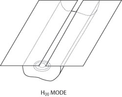
Fig. 1 Ground plate with a slot backed by a cylinder.
Introduction
The antenna was developed by two of the authors of this paper.1,2 In their original work, the antenna was manufactured using a machined assembly approach. They also measured simple arrays in various configurations. One of the major advantages of the design is that it is amenable to standard PCB production. This type of antenna should be of interest to the wireless community where issues of the antenna’s cost, bandwidth and gain are all important drivers. The current state of the investigation is to find an optimal array design using the antenna.
The second part of this article shows how the design tools were used to come up with good candidates for the array design. Investigations include optimizing the array’s directivity, return loss and bandwidth. For optimal performance, the array needs both optimized layouts of the corporate feed and the antenna itself. AXIEM, AWR’s 3D planar EM simulator, was used to optimize the performance of the antenna and antenna feed design. Variables were used to control the layout of the antenna, allowing the layout of the antenna to be optimized directly in EM simulation. An alternative approach would be to develop a user defined EM model, in which the data points are automatically obtained from EM simulation. The circuit simulator would then use interpolation when calling the database to get any required set of parameter values.3

Fig. 2 Front (a) and rear (b) views of the original antenna.
Basic Antenna Operation
The basic operating principle of the antenna is shown in Figure 1. Slot antennas are widely used in planar environments. The limitation in their performance is the length of the slot, which is typically required to be less than half a free space wavelength, thereby limiting their radiation efficiency. Cavities are used to back the slot for two reasons: first, it prevents radiation from the bottom of the slot, and second, it increases the gain at the waveguide resonance. Unfortunately, a cavity also decreases the bandwidth of the antenna. The antenna used here uses a waveguide instead of a cavity. In particular, the two ends of the waveguide are left open. There is therefore no cavity resonance to restrict the bandwidth. At the same time, the dominant waveguide mode, the H00 mode,4,5 allows for a longer slot, up to almost a wavelength. This helps the gain and efficiency of the antenna.
The performance of the antenna has been experimentally verified for both single slots, as well as arrays of two and four slots. In the original investigation, the antennas were constructed by mechanically attaching the waveguides, as shown in Figure 2.

Fig. 3 Return loss (a) and gain (b) for the single element antenna.
The antenna was manufactured using 30 mil RO4350B laminate with a ground plane size of 60 × 60 mm. The slot has dimensions of 2 × 44 mm. The slot length is 0.8 wavelengths long at the frequency of operation, 5.4 GHz. The waveguide has horizontal dimensions of 18 × 40 mm, and a depth of 11 mm. The experimental results were encouraging. For example, Figure 3 shows the return loss and gain of the antenna. Assuming a design goal of 13 dB return loss, the bandwidth of the antenna is about 10 percent, with gain of about 9.8 dB in the center of the band.
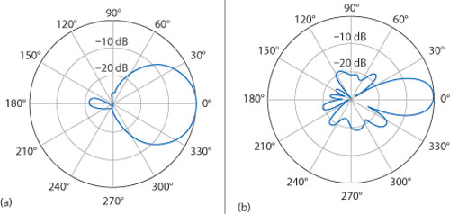
Fig. 4 Field patterns for the four-element array: horizontal plane-perpendicular to the slots (a) and vertical plane-parallel to the slots (b).
Various array configurations were then tried. For example, Figure 4 shows the E and H antenna patterns for a four-element array. The array was designed to operate at 2.4 GHz. The four slots were parallel to each other with a half wavelength distance between them. A corporate feed was etched on the opposite side of the substrate, which for this experiment was 40 mil RO4350B laminate. The antenna efficiency compared to the theoretical maximum, which can be achieved for the given aperture with uniform field distribution, is over 94 percent.
One of the advantages of this type of antenna is that the slots are isolated from each other to a much greater degree than a normal slot antenna array. Measurements show isolation better than {30 dB between elements.

Fig. 5 A single slot and waveguide drawn in AXIEM.
Optimizing the Design
The performance of the antenna array depends on a number of critical parameters:
- The layout of the feed network.
- Slot size and waveguide dimensions.
- Substrate thickness and dielectric constant.
The EM simulation tool was used to perform the parametric studies and performance optimization, in this case: return loss, bandwidth and gain. The 3D planar EM analysis performed by AXIEM is well suited to this type of antenna study. First, it is not enclosed in a box, making it a natural fit for planar antenna problems. Second, the planar nature of the antennas geometry lends itself well to a 3D planar simulator. The antenna consists of horizontal metal and the vertical walls of the cavity. In PCB technology, the vertical walls will probably be a tightly packed row of vias that can be included in the EM simulations (although this was not tried in this study). The decision was made to use a planar simulator rather than a full 3D EM simulator to avoid the use of radiation boundary conditions at the edge of the meshing domain that can increase the simulation time. In our experience, planar simulators will be faster for this type of geometry, and because we are optimizing, speed of simulation is an important factor.
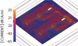
Fig. 6 Currents for a two-slot corporate- fed array.
The first group of simulations looked at the physical geometry of the antennas themselves. A simple preliminary layout is shown in Figure 5. A single slot was studied. Note that the feed of the antenna has been simplified. Port 1 is a simple internal port across the middle of the slot. Later studies looked at a more realistic feed network. Parameters varied and included the slot width, length and waveguide dimensions. There are a variety of ways to control the optimization in the design environment, including Microwave Office (MWO). AXIEM has the capability of using parameters to control the drawing of the EM layout directly. Therefore, the various widths and lengths of the slot and waveguide can all be controlled by a few parameters, which in turn are optimized. Either the parameters themselves are run through an optimizer, which is very time consuming as an EM simulation is required at each step of the optimization, or an EM-based model is created in which the parameters are swept over a reasonable number of steps and the optimizer is then run on the model. For this example, the model approach was used.
The goals in the next phases of the study were to array the slots, and to design the corporate feed network. The corporate feed network was created in the MWO schematic editor using models and optimized in the conventional manner. The layout was then automatically exported to AXIEM using the EM extraction technology. In this manner, the layout from the schematic (the corporate feed) and EM drawings (the slots and waveguides) can be combined easily without the need for a manual redraw. The current distribution for a two-slot corporate fed array is shown in Figure 6.
The currents show the optimized corporate feed on an inner layer of the substrate. Note that the current distribution on the lengths of slot is relatively uniform, which is one of the important design goals of the antenna. The slots were 2.7 × 108 mm long on a 30 mil thick substrate with a dielectric constant 3.45. This makes the slots 0.8 wavelengths long at the frequency of operation 2.45 GHz.
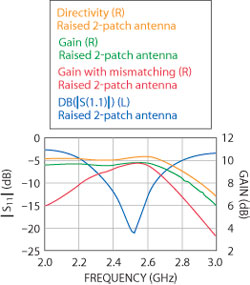
Figure 7 Return loss and gain of the dual- slot antenna.

Figure 8 Radiation patterns for the two-element array.
Figure 7 is a sample of the results obtained for this example, the return loss and gain of the antenna. Note that the |S11|<-12 dB and the gain and directivity are relatively flat over the range of operation, from 2.4 to 2.6 GHz. Figure 8 shows the radiation patterns for the array.
The final example shows the isolation between the various slots. Figure 9 shows four slots, grouped into two of the dual-slot antennas studied in the previous example. Each of the dual-slot antennas is again fed by a corporate feed. The designers were concerned about coupling between the two groups of elements. A high level of coupling would degrade the performance of the array.
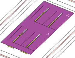
Fig. 9 Two-coupled dual-slot antenna.
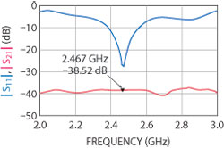
Fig. 10 Mutual coupling between the dual-slot antennas.
Figure 10 shows the coupling between the two groups of antennas. It is about {38 dB at the frequency of operation. This is significantly lower than the coupling that would occur without the waveguides. Figure 10 also shows the return loss of one of the dual-slot antennas not be degraded by the presence of the other antenna.
The antenna can be used as a principal radiating element in low, medium and high gain directional panel antennas as well as a basic element in base station or smart antenna designs. The antenna is suitable for MIMO applications because of good isolation, below -35 dB, and frequency range of the antenna impedance match is up to 22 percent (|S11|<−10 dB). The antenna is easy to manufacture using conventional PCB technology. Active components such as phase shifters, amplifiers, or switches can be easily integrated in the antenna feeding network.
Conclusion
A waveguide-backed slot antenna array was simulated and optimized using the 3D planar EM simulator, AXIEM and MWO design environment. New software capabilities allow the designer to use parameters in the layout to directly optimize shapes or to create EM- based models, which can in turn be optimized. The design environment allows schematic layout to be sent directly to the EM simulator. In this example, the corporate feed was optimized using models in the schematic, whereas the antenna was optimized directly in the EM simulator. Therefore, maximum simulation efficiency was obtained. Models were used where available, and direct EM optimization was used where they were not.
References
- A.V. Sulima and V. Veremey, “Transmission Line Slot Antenna,” Patent Application Pub. No. US 2011/0090128 A1 (granted in 2012).
- A.V. Sulima and V. Veremey, “A Highly Efficient Slot Antenna,” 2010 IEEE AP-S International Symposium on Antennas and Propagation, Toronto, ON, Canada, July 2010.
- For information on AWR, Microwave Office and AXIEM - http://web.awrcorp.com.
- V. Veremey, “Superdirective Antennas with Passive Reflectors,” IEEE Antennas and Propagation Magazine, Vol. 37, pp. 16-27, 1995.
- A.V. Sulima, “Scattering of TE Waves by Cavity Backed Slots,” Proceedings of the 32nd European Microwave Conference, 2002, Milano, Italy.