
Amplifier designers have been making use of modern transistor models since their first appearance in the mid-1970s. Models have allowed engineers to create advanced designs with first-pass success, without the need for multiple prototypes and design iterations. But with so many different modeling techniques, how does one select which one to use? The three most common types of models used in industry today are: physical models, compact models and behavioral models.
Physical models, as their name suggests, are based on the physics of the device technology. These models are dedicated to the transistor itself and not the overall circuit. Due to the nature of the model, complex model equations have to be used, which can lead to time-consuming simulations. The advantage of the physical model is that it can be successfully used over the largest operating range, compared to alternate methods, since equations are used to describe complex physical rules rather than actual measurement results.
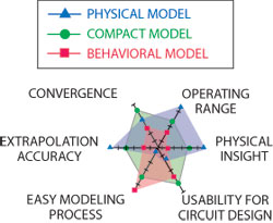
Fig. 1 Type of large-signal models.
Compact transistor models, based on measured IV and S-parameters, allow designers to shift focus from transistor designs to circuit designs. Extracted from quasi-isothermal pulsed IV and pulsed S-parameter data and validated with load-pull characterization, compact transistor models contain a reduced set of parameters. Unlike other model types, compact models take into account complex phenomena, such as electro-thermal and trapping effects. For simulations under nonlinear operating conditions, responses to complex modulated signals (such as EVM or ACPR) are accurately predicted as low-frequency and high-frequency memory effects are taken into account. Compact transistor models are ideal for die-level applications, as developing such a model from IV and S-parameters is straightforward and relatively quick. Packaged-transistor models need to include a die-level model as well as a bonding model and package model, and consequently can be time consuming and costly.
Behavioral models, based on frequency domain measurements, are far less flexible than physical or compact transistor models, but can be easily developed for any type of component (including die-level or packaged transistors). Behavioral models are considered “black-box” models, where only the responses of the component to some controlled stimuli are known, and are consequently only valid under the operating conditions measured. This model type is actively under development and has been recently improved to take into account memory effects,1,2 however, as a table-based model, it cannot be as complete as a formula-based model.
It is clear that each model type, physical, compact and behavioral, has unique advantages and disadvantages, as illustrated in Figure 1. While there is no one-size-fits-all model, compact transistor models offer the shortest development time for maximum flexibility with regard to die-level transistors.
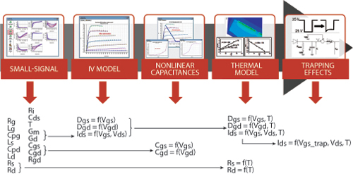
Fig. 2 Compact FET model extraction flow.
Research and development of compact transistor models has been, and continues to be, an important topic for universities and institutes across the globe.3-9 As such, an abundance of literature and documentation exists on the background R&D of compact models. This discussion will concentrate on the main topics involved with model extraction of wide band gap (WBG) field effect transistors (FET) such as gallium nitride (GaN) FETs. The perfect GaN compact transistor model needs to be accurate for device operation over temperature, bias and RF power. The design flow of a GaN FET compact transistor model, shown in Figure 2, consists of:
- Linear model extraction through small-signal S-parameters
- Nonlinear model extraction through pulsed IV measurements
- Nonlinear capacitance modeling through synchronized pulsed IV/RF
- Electro-thermal modeling through temperature control
- Trapping effect modeling
Additionally, the compact transistor model can be validated through load-pull measurements.
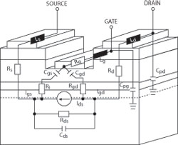
Figure 3 Compact FET model schematic.
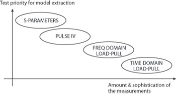
Figure 4 Measurements for compact model.
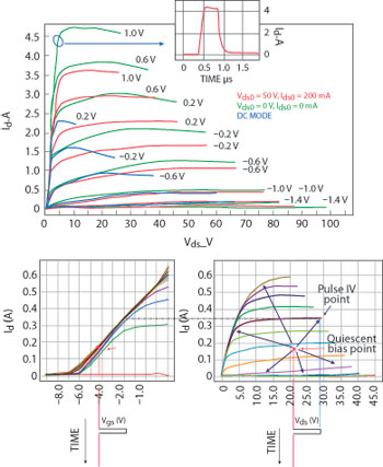
Fig. 5 DC and pulsed IV characteristics.
Linear Model Extraction
The first step in linear model extraction is to use S-parameters to determine the transistor’s extrinsic parasitic elements (Rg, Lg, Cpg, Rd, Ld, Cpd, Rs and Ls), as sketched in Figures 3 and 4. By defining a set of extrinsic elements, the S-parameter data can be de-embedded to the intrinsic reference plane and a set of intrinsic parameters (Cgs, Cgd, Gm, Gd, Cds, Ri, Tau, Rgd) can be extracted using explicit equations.10-11
During the optimization process, the goal of the linear modeling step is to determine values for the extrinsic parameters, which in turn provides a set of intrinsic parameters with a fixed value versus frequency. During the modeling optimization, measured and modeled S-parameters are compared over the entire RF bandwidth. The measured S-parameters are converted to the corresponding [Y] and [Z] parameters, so that both [Y] and [Z] parameters can be compared at both intrinsic and extrinsic reference planes.
Nonlinear Model Extraction with Pulsed IV
Nonlinear model extraction uses pulsed IV measurements to study the effects of temperature-dependent performance (including self-heating) in safe operating regions and to study the breakdown area of the transistor (see Figure 5).12 Pulse widths are kept sufficiently short in order to avoid a strong temperature variation during the pulse duration and the duty cycle is kept sufficiently low in order to avoid a mean variation of the temperature, so that the transistor’s pulsed IV measurements are obtained under quasi-isothermal operating conditions.
It is necessary to determine the transistor’s thermal impedance in order to complete an electro-thermal model that can dynamically predict performance as a function of device temperature (chuck temperature) and self-heating.9,13 To extract the thermal impedance, two sets of measurements are performed.
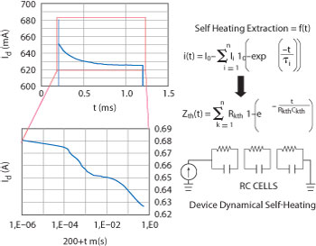
Fig. 6 Thermal model extraction.
First, IV measurements are performed under both continuous (DC) and short-pulsed conditions in order to extract the thermal resistance. As shown in Figure 6, longer pulses are then applied in order to study the current decrease with time and extract the thermal capacitance. How the temperature (and therefore performance) varies with time is related to the transistor’s design, number of layers, type of carrier, heat sink, etc.; the thermal impedance can be modeled by a combination of several thermal resistances and several thermal capacitances representing various time constants. This thermal circuit provides the equivalent transistor junction temperature as a function of DC power and is used in the various sub-circuit models (resistances, current source, diodes and breakdown circuits) that are linked to voltages, currents and temperatures.
In the example shown in Figure 7, the input current diodes must be modeled by equivalent nonlinear current sources that are able to generate a positive gate current when the transistor is biased in forward model with low Vds and high Vgs values, and able to generate a negative current for high Vds and pinch-off Vgs values. To ensure convergence, the output current source model has to be continuous at n-order for any Vgs and Vds values. The AMCAD-FET model uses a current source model that can be formulated using the following equations:
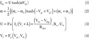
where α1, α2, Vgs1, I1, λ, Vdsp and Rds0 are parameters. The “Fa” function defines a lower limit to a related function from an arbitrary value U0 with an adjustable smooth transition parameter Ru. The “Fp” function is an n-order polynomial with two variables (Vgs, Vds). Additionally, measurements can be repeated at various chuck temperatures when measuring on-wafer. This allows a temperature-dependence variable to be determined and applied to the model.
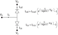
Fig. 7 Gate current model.
Nonlinear Model Extraction with Pulsed IV/Pulsed RF
Nonlinear capacitance modeling, determining Cgd and Cgs models, is achieved through synchronized pulsed RF (Pulsed S-parameters) and pulsed bias (Pulsed IV) measurements along with the predicted RF load line. While nonlinear capacitances can be modeled by equations that depend on both Vgd and Vgs voltages concurrently (referred to as two-dimensional models), it has been shown that one-dimension capacitance models are more robust regarding convergence without sacrificing accuracy.14 The Cgd capacitance model is therefore linked with Vgd while the Cgs capacitance model relies on Vgs.
The feedback capacitance Cgd depends heavily on the drain voltage; therefore, it must be included to fit large-signal operating conditions. The Cgd capacitance model is defined by the equation
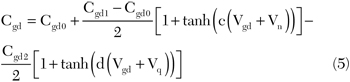
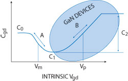
Fig. 8 Cgd nonlinear capacitance.
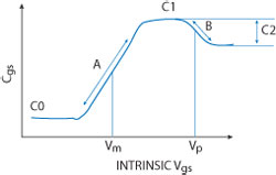
Fig. 9 Cgs nonlinear capacitance.
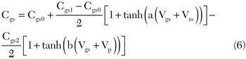
This one-dimension Cgd capacitance model, shown in Figure 8, was initially optimized for gallium arsenide (GaAs) transistors, but has been updated for GaN technologies. Along the same RF load line, the one-dimension input capacitance model Cgs, shown in Figure 9, depends heavily on gate voltage. The gate voltage’s nonlinearity greatly affects the model’s harmonic response. The capacitance can be modeled by the equation
The output capacitance Cds is linear; no voltage dependence is taken into account due to the weak influence for amplification purposes.
Trapping Effects
Nonlinear model extraction also takes advantage of pulsed IV measurements to isolate the trapping effects as a function of quiescent bias condition. Trapping effects are parasitic effects that reduce the maximum output current; the charging and discharging of traps influences Ids and leads to current collapse. Trapping corresponds to the existence of energy states, which can be occupied by holes or electrons in the gap. These holes or electrons are trapped at these levels over a time period and cannot take part in conduction, hence the term trap. Trapping is the result of impurities or defects in the crystalline network of the material from which the transistor is composed, and alters the electric behavior of the transistor at microwave frequencies.
Pulsed IV measurements are used to study the individual trapping effects and differentiate between surface trapping (gate-lag) and buffer trapping (drain-lag). When performing pulsed IV measurements, it is important to ensure the IV pulses are shorter than the emission time constant of the traps. It is also important to maintain a constant temperature throughout the measurement to be certain that the device changes are due to trapping effects and not temperature changes.
Gate-lag is mainly attributed to surface trapping effects. In order to isolate these effects, two series of measurements are made with identical dissipated powers equal to zero. When performing pulsed IV measurements, the two quiescent bias points chosen are:
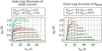
Fig. 10 Trapping effects.
QP1 : Vgs0 = Vp, Vds0 = 0 V
QP2 : Vgs0 = 0 V, Vds0 = 0 V
Vp is the pinch-off voltage applied on the gate. Because both dissipated powers are zero, any difference between IV characteristics can be attributed to the presence of gate lags.
Drain-lag is mainly attributed to buffer trapping effects. In order to isolate these effects, two series of measurements are made with identical dissipated powers equal to zero. When performing pulsed IV measurements, the two quiescent bias points chosen are:
QP1 : Vgs0 = Vp, Vds0 = 0 V
QP3 : Vgs0 = 0 V, Vds0 >> 0 V
Examples of typical gate-lag and drain-lag IV curves are shown in Figure 10.
These parasitic phenomena can be modeled by a trapping circuit composed of gate- and drain-lag sub-circuits that are connected to the gate command15 in order to drive the output current as a parasitic phenomenon. The lagging hysteresis can be modeled by a circuit that contains a diode element that will reproduce the dissymmetry between the capture and emission times.16
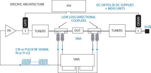
Fig. 11 VNA-based load pull setup.
Load-Pull for Model Validation
Load-pull measurements are used to validate compact transistor models beyond 50 Ω by varying the impedances presented to the transistor and comparing measured and modeled parameters. In order to achieve a good correlation between measured and modeled results, it is important to use a vector-receiver (real-time) load-pull system, as shown in Figure 11. Vector-receiver load-pull systems make use of a vector receiver calibrated at the device-under-test (DUT) reference plane to measure the transistor’s large signal input impedance.17 Knowledge of the transistor input impedance removes the mismatch effect between the source impedance and the device impedance, allowing for a true power gain comparison. Power gain is directly related to the intrinsic transistor’s performance contained within the model, whereas transducer gain is only an indicator of how the transistor is matched. The mismatch between the source impedance and the transistor’s input impedance can hide unstable operating conditions where the transistor’s input impedance has negative values for certain load impedances,18 as the input impedance varies with power delivered to the input of the transistor. This input impedance measurement is important for model validation; during simulations, a model’s effectiveness is judged by its ability to accurately predict power gain expansion and/or compression, which plays a major role in linearity.
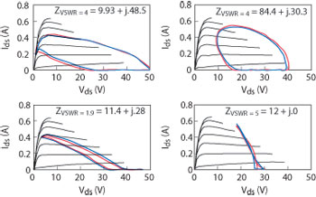
Fig. 12 Model validation.
Time-domain load-pull measurements may also be used for model validation.19 In addition to the parameters obtained from a frequency-domain system, time domain load-pull allows for the measurement of voltage and current waveforms and load lines. When correctly calibrated and de-embedded to the intrinsic transistor reference plane, the RF load line can be displayed and superimposed onto the transistor’s IV characteristics, and a comparison between measured and modeled results can be made, as shown in Figure 12. Time-domain voltage and current waveforms and load lines can be used to verify whether the transistor is operating close to RF breakdown, or used to confirm class of operation (A, AB, C, E, F, F-1, G…).
Conclusion
Amplifier designers are under more stress than ever to release effective products in the least amount of time and maximize profitability; meaning first-pass design success and being first-to-market. Gone are the days when engineers could cut and paste, design by trial and error, and work at their own pace to release innovative products. Compact transistor models are the first and most crucial step in a successful MMIC design flow and, when used in conjunction with circuit simulators, can lead to first-pass design success and first-to-market.
References
- W. Demenitroux, C. Maziere, T. Gasseling, B. Gustavsen, M. Campovecchio and Q. Quéré, “A New Multi-Harmonic and Bilateral Behavioral Model Taking Into Account Short Term Memory Effect,” 2010 European Microwave Conference Digest (EuMC), pp. 473-476.
- J. Verspecht, J. Horn and D.E. Root, “A Simplified Extension of X-Parameters to Describe Memory Effects for Wideband Modulated Signals” 2010 IEEE Microwave Measurements Conference Digest (ARFTG), pp. 1-6.
- M. Rudolph, C. Fager and D.E. Root, Nonlinear Transistor Model Parameter Extraction Techniques, The Cambridge RF and Microwave Engineering Series, Cambridge University Press, Cambridge, U.K., 2012.
- P. Aaen, J.A. Pla and J. Wood, Modeling and Characterization of RF and Microwave Power FETs, The Cambridge RF and Microwave Engineering Series, Cambridge University Press, Cambridge, U.K., 2007.
- L. Dunleavy, C. Baylis, W. Curtice and R. Connick, “Modeling GaN: Powerful but Challenging,” IEEE Microwave Magazine, Vol. 11, No. 6, October 2010, pp. 82-96.
- G. Avolio, D. Schreurs, A. Raffo, G. Crupi, I. Angelov, G. Vannini and B. Nauwelaers, “Identification Technique of FET Model Based on Vector Nonlinear Measurements” IET Journal, Electronics Letters, Vol. 47, No. 24, 2011, pp. 1323-1324.
- W.R. Curtice, “Nonlinear Modeling of Compound Semiconductor HEMTs State of the Art,” 2010 IEEE MTT-S International Microwave Symposium Digest, pp. 1194-1197.
- I. Angelov, H. Zirath and N. Rorsman “A New Empirical Model for HEMT Devices,” 1992 IEEE MTT-S International Microwave Symposium Digest, Vol. 3, pp. 1583-1586.
- C. Charbonniaud, A. Xiong, S. Dellier, O. Jardel and R. Quéré, “A Nonlinear Power HEMT Model Operating in Multi-bias Conditions,” 2010 European Microwave Integrated Circuits Conference Digest (EuMIC), pp. 34-137.
- M. Berroth and R. Bosch, “High-Frequency Equivalent Circuit of GaAs FETs for Large-Signal Applications,” IEEE Transactions on Microwave Theory and Techniques, Vol. 39, No. 2, February 1991, pp. 224-229.
- G. Dambrine, A. Cappy, F. Heliodore and E. Playez, “A New Method for Determining the FET Small-Signal Equivalent Circuit,” IEEE Transactions on Microwave Theory and Techniques, Vol. 36, No. 7, July 1988, pp. 1151-1159.
- J.P. Teyssier, P. Bouysse, Z. Ouarch, D. Barataud, T. Peyretaillade and R. Quere, “40 GHz/150 ns Versatile Pulsed Measurement System for Microwave Transistor Isothermal Characterization,” IEEE Transactions on Microwave Theory and Techniques, Vol. 46, No. 12, December 1998, pp. 2043-2052.
- J.A. Lonac, A. Santarelli, I. Melczarsky and F. Filicori, “A Simple Technique for Measuring the Thermal Impedance and the Thermal Resistance of HBTs,” 2005 European Gallium Arsenide and Other Semiconductor Application Symposium Digest, EGAAS, pp. 197-200.
- S. Forestier, T. Gasseling, P. Bouysse, R. Quéré and J.M. Nebus, “A New Nonlinear Capacitance Model of Millimeter Wave Power PHEMT for Accurate AM/AM–AM/PM Simulations,” IEEE Microwave and Wireless Components Letters, Vol. 14, No. 1, January 2004, pp. 43-45.
- N. Matsunaga, M. Yamamoto, Y. Hatta and H. Masuda, “An Improved GaAs Device Model for the Simulation of Analog Integrated Circuit,” IEEE Transactions on Electron Devices, Vol. 50, No. 5, May 2003, pp. 1194-1199.
- O. Jardel, F. De Groote, T. Reveyrand, C. Charbonniaud, J.P. Teyssier, D. Floriot and R. Quéré, “An Electrothermal Model for AlGaN/GaN Power HEMTs Including Trapping Effects to Improve Large-Signal Simulation Results on High VSWR,” IEEE Transactions on Microwave Theory and Techniques, Vol. 55, No. 12, December 2007, pp. 2660-2669.
- S. Dudkiewicz, “Vector-Receiver Load-Pull Measurements,” Microwave Journal, Vol. 54, No. 2, February 2011, pp. 88-98.
- T. Gasseling, D. Barataud, S. Mons, J.M. Nebus, J.P. Villotte and R. Quéré, “A New Characterization Technique of Four Hot S-Parameters,” 2003 IEEE MTT-S International Microwave Symposium Digest, Vol. 3, pp. 1663-1666.
- F. De Groote, J.P. Teyssier, T. Gasseling, O. Jardel and J. Verspecht, “Introduction to Measurements for Power Transistor Characterization,” IEEE Microwave Magazine, Vol. 9, No. 3, June 2008, pp. 70-85.