
Inkjet-printed and nanotechnology-enabled flexible antennas, RF electronics and sensors fabricated on paper and polymer substrates (e.g. Liquid Crystal Polymer (LCP), Kapton®) are introduced as a system-level solution for ultra-low-cost mass production of communication, Radio Frequency Identification (RFID) Tags and Wireless Sensor Nodes (WSN) in an approach that could be easily extended to other microwave and wireless applications. The review will cover examples from UHF up to the millimeter-wave frequency ranges (mmID). This article will cover the state-of-the-art area of fully-integrated conformal wireless sensor modules on paper or flexible LCP, and demonstrate the first 2D/3D wireless sensor integration with an RFID tag module on paper, as well as numerous 3D multilayer paper-based and LCP-based RF/microwave structures that could potentially set the foundation for convergent wireless sensor ad-hoc networks of the future with enhanced cognitive intelligence and "rugged" packaging.
Eco-friendly Paper Substrate
Paper is an organic-based, inexpensive and flexible substrate. It is widely available and one of the cheapest materials for mass production in the industry.1 Plus, it is not only environmentally friendly but also suited for reel-to-reel processing. In addition, paper can be hydrophobic and/or fire-retardant by adding certain textiles to it.2 In addition, paper is suited for fast printing processes and direct write methodologies like inkjet printing techniques instead of the traditional metal etching techniques to maximize its cost efficiency. This is because inkjet printing directly deposits metals on the desired place while traditional metal etching techniques remove metals during etching that are not renewable. Therefore, a fast process like this can be used efficiently to print electronics on paper substrates. RF characterization of the paper substrate and conductive ink for inkjet printing is essential to build high frequency circuits and antennas using these techniques. A number of paper-based materials are available commercially at low costs with varying properties such as density, coating, thickness and weight for a wide variety of applications such as printing, photography, packaging, etc. Choosing the correct paper material for use as a substrate requires careful selection based on the paper's response to the propagating microwave fields and robustness to the fabrication process.
Paper substrates for inkjet printing purposes should be hydrophilic and heat-resistant. In addition, it is commercially available to enable mass production. The conductive ink cannot attach on the surface if it is highly hydrophobic, while it cannot form a conductive solid metal if the paper cannot withstand certain temperatures. In the previous works, commercially available photo paper fulfilling the above conditions and its electric properties are studied.3-5
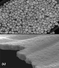
Figure 1 Inkjet-printed nano-silver ink (a) before sintering (b) sintering at 180°C for 10 minutes.
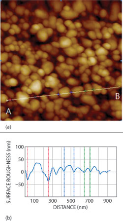
Figure 2 (a) Surface image in the area of 1 µm by 1 µm; (b) surface profile of line AB.
Conductive Inkjet Printing
The conventional masks for traditional etching techniques for fabrication are not necessary for inkjet printing since it is a direct-write technology, which means that designed circuit pattern is transferred to the substrate without any byproducts.4 Therefore, dangerous chemicals, such as etchants are not needed, which make it an environmentally friendly fabrication process. The nano-silver ink used has high conductivity when it is printed and sintered since silver has the highest electrical conductivity among all of the metals. To remove the solvent in silver ink and impurities from the printing process, the sintering process is required after printing. In addition, the bond between the deposited silver ink and the substrate can be improved by the sintering process. The conductivity of the silver ink after sintering varies from 4 to about 16 mW-cm, which is about 2.5 to 10.1 times higher than bulk silver's resistivity, which is dependent on sintering time and temperature.6 Figure 1 shows a Scanning Electron Microscope (SEM) image of nano-silver ink before/after sintering at 180°C for 10 minutes. Figure 2 shows a surface image of printed nano-silver ink from Atomic Force Microscopy (AFM), which is sintered at 120°C for four hours. The measured roughness based on the arithmetic average of absolute values (Ra) is 11.4 nm, root mean squared value (Rq) is 14.4 nm and the grain size after sintering at 120°C varies from about 20 to 200 nm. The roughness of the inkjet printed metal is very small so that the inkjet printing technique can be applied to mm-wave applications in the future.
Inkjet Printed Antennas
Based on previous characterization of the paper substrate and nano-silver ink, many types of devices and circuits were designed and fabricated using inkjet printing techniques and integrated into wireless sensor systems and modules. Among many applications, inkjet printing techniques are mainly applied to RFID technology due to their low cost and mass production features.
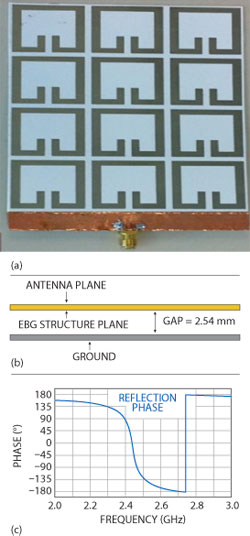
Figure 3 (a) Inkjet-printed 4×3 EBGs, (b) integrated antenna, EBGs and ground plane and (c) phase response of reflected wave.
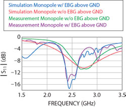
Figure 4 S11 of the fabricated antenna on the EBGs.
Recently, the use of the inkjet printing technology has been broadly extended in the area of integrated antennas up to the millimeter-wave (mm-wave) frequencies. For instance, the feasibility of inkjet printed antennas for various applications, such as Ultra-Wideband (UWB) and mm-wave modules on LCP and integrated power scavenging topologies have been studied.7-10 Among the plethora of applications, one of the most recent efforts focuses on the inkjet printing of an Electromagnetic Band Gap (EBG) structure for wearable sensors. In previous efforts, a dipole antenna was placed above the inkjet printed EBGs to increase the gain for low-proximity ground planes.11 In this case, the EBGs and ground plane form an Artificial Magnetic Conductor (AMC), and the reflected waves from the AMC constructively interfere with the radiated waves over the designated frequency band. EBGs are designed using single ring resonators instead of split ring resonators by an inkjet printing technique.12 Figure 3a shows an inkjet-printed 4×3 resonator array. Figure 3b shows the integrated topology of an integrated monopole antenna, EBGs and ground plane. Figure 3c shows the phase response of the designed EBGs, demonstrating reflected phase values within the range within -90 to about +90 degrees verifying constructive interference. Figure 4 shows the measured S11 of the antenna. The EBG-backed antenna shows a better performance than the antenna without EBGs. The simulated and measured radiation patterns are shown in Figure 5. The most notable difference is the gain of the designed antenna. The gain of the EBG-backed antenna is 0.95 dBi, while the antenna without EBGs on the ground plane is -4.6 dBi. The gain is increased by 5.5 dBi and this type of antenna can be placed on any kind of material (e.g., conductive surfaces, human body, liquid containers) since the EBGs over the ground plane virtually isolate the antenna system from the ambient environment.
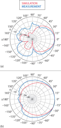
Figure 5 Radiation patterns at 2.45 GHz (a) E-plane and (b) H-plane.
As a next step, this antenna was integrated with a commercially available wireless temperature sensor in order to demonstrate its applicability to wearable wireless biosensors. The inkjet-printed EBG-backed antenna has tripled the communication range of the sensor from 29.5 to 82.8 m. This prototype verifies the capability of the inkjet printing technology to seamlessly integrate into conventional technology.
Inkjet Printed 2D Active Wireless Sensor Modules
To verify the module-level integration feasibility of this approach, a low- power active (battery-powered) RFID-enabled wireless temperature sensor tag was designed on paper ("System-on-Paper") to operate at 900 MHz. The power, digital and RF transmission lines/traces in the design were formed by the sintered nano-based ink that was deposited using the inkjet printing process on a paper-based substrate. The basic system comprised of a commercial microcontroller unit (MCU) that was used to sample a commercial temperature sensor and broadcast its information out by modulating a phase locked loop (PLL) module in a wireless transmitter integrated in the same chip as the microcontroller unit. The battery, temperature sensor and MCU/wireless transmitter IC were mounted on the inkjet-printed nano-particle-based traces using a conductive silver epoxy due to the low temperature tolerance of paper to the heat generated by a soldering iron.13,14
The signals used in the circuit included the high-speed digital signals used in the clocking of the MCU with an external crystal oscillator and the base-band signals used by the MCU to modulate the PLL in the integrated transmitter. In addition, 900 MHz amplitude-shift-keyed (ASK) and frequency-shift-keyed (FSK) signals between 860 and 925 MHz, similar to those required by the UHF Gen-2 protocol,15 were output by the transmitter's PA into a UHF antenna also fabricated using the same conductive ink. To ensure maximum conductivity and antenna efficiency, the entire circuit was printed over with 12 layers of silver nano-particle ink resulting in a conductor thickness of 12 microns. The concentration of the silver nano-particles in the different traces was accurately controlled to achieve the optimum tradeoff between precision and conductivity for the different signals in the circuit. A higher precision inkjet cartridge spraying 1 picoliter droplets was used to print finer areas in the circuit layout, such as the digital MCU traces (~150 microns wide), and a 10 picoliter cartridge was used to print larger areas on the antenna and the RF ground planes/traces in the circuit layout to further increase conductivity. The final prototype developed can be seen in Figure 6.13
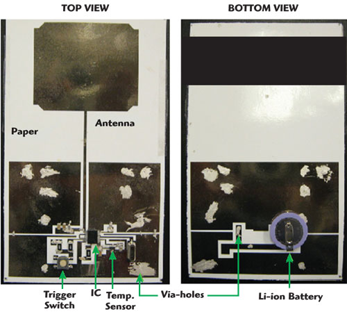
Figure 6 Wireless sensor module prototype circuit developed on paper using inkjet printing of the silver nanoparticle-based conductor.
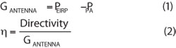
The simulated gain of the monopole antenna printed using the silver nano-particle based ink was a maximum of 2.6 dBi, as shown in the simulated radiation pattern in Figure 7. The transmitted signal as captured by a Real Time Spectrum Analyzer attached to an RFID antenna on the receiver side is shown in Figure 8 verifying the operation of the wireless sensor module. From the captured power in Figure 7, the effective isotropic radiated power (PEIRP) from the wireless sensor circuit was determined to be 4.91 dBm,13,16 which translates into a radiation efficiency of 61 percent for the silver nano-particle based antenna using Equation 1:
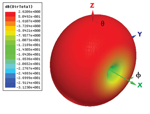
Figure 7 Simulated radiation pattern of the monopole antenna.
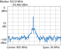
Figure 8 Wireless sensor module prototype circuit developed on silver nanoparticle-based conductor on paper using inkjet printing.
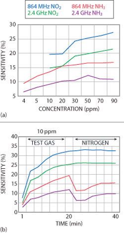
Figure 9 (a) Response as a function of concentration taken after stabilization and (b) timing response for NH3 and NO2 using concentration of 10 ppm at 864 MHz and 2.4 GHz.
where PEIRP = effective isotropic radiated power (4.91 dBm = 3.097 mW), PPA = power amplifier output fed into the antenna (4.5 dBm = 2.81 mW), GANTENNA = antenna gain and Directivity = Antenna directivity (~2.6 dBi).
Battery-less Inkjet-Printed Carbon Nanotube Sensors
Further work was done to evaluate the performance of inkjet-printed carbon nanotubes (CNT) as a zero power, battery-less, remote sensor. The idea was to use the ion-exchanging behavior of the CNTs with ambient gases as a mechanism to sense the chemical content in them. The varying electrical properties of the CNTs, due to their ability to absorb certain chemicals, present in the gases can be remotely interrogated and measured by embedding them as gas-sensitive loads of specially designed antennas. An optimized recipe that can be easily realized on various flexible substrates using inkjet printing was used. Chemical absorption produces changes in the properties of CNT embedded antenna structures, such as real and imaginary impedance, DC resistance, conductance and effective dielectric constant. These changes can be used to determine the presence of various chemical compounds by translating the material effects into measurable electrical quantities such as changes in measurable voltage, current and resonant frequency.17 As a first step in the development of such zero power remote CNT sensors, stable carbon nanotube and graphene-based inks capable of integration in a wide range of potential devices via common ink-jet printing methods have been developed.17 Based on these inks, several devices have been produced.
Sensor Type 1: RF Responsive CNT as a Chemical Sensing Element
In order to study the RF response of the CNT to the different chemical gas concentrations, several samples of the microstrip waveguides embedded with single- and multi-walled (MWCNT) molecules were fabricated using inkjet printing technology. The sensitivity of each sample to the gases is shown in Figure 9. Sensitivity is defined as the change of the CNT structure's impedance in the presence of the test gas relative to air (or other controlled environment). The CNT embedded microstrip line's response for gas concentration and the material's timing response were taken at room temperature and impedance measurements of 75-layer MWCNT samples were taken in air and in the presence of different NH3 and NO2 concentrations, i.e., 10, 15, 20, 30, 50, 70 and 90 ppm, across a range of frequencies from 50 MHz to 3 GHz.
Figure 9 shows the change in sensitivity as a function of concentration for both gases at the non-licensed spectrum bands of 864 MHz and 2.4 GHz. Sensitivity of 21.7 percent and 9.4 percent was achieved for 10 ppm NO2 and 4 ppm NH3, respectively, at 864 MHz, which is higher than that achieved in recent works18,19 for higher concentration (100 ppm) of NH3. Figure 9b provides the timing response to the same chemical gases at the chosen frequencies. For this portion of the experiment, 10 ppm was used as the concentration for both gas tests. The measurements were taken at 1, 2, 5, 10, 15 and 20 minutes. As shown in Figure 9b, the MWNT-based gas sensor demonstrates fast response to both gases (few seconds); the sensitivity achieved at 864 MHz is 24.2 percent for NO2 and 12.7 percent for NH3 in just two minutes. Note that after testing, the sensor exposed to NH3 shows more rapid recovery, possibly due to the greater electro-negativity of one pole of the NH3 molecule.
Sensor type 2: Inkjet Printed CNT Embedded Antennas as a Battery-less Remote Wireless Sensor
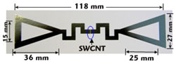
Figure 10 Inkjet-printed CNT antenna sensor prototype embedded with SWCNT film on a flexible paper substrate.
With the inkjet printed CNT structure impedance response showing a measured variability in the presence of gases, a battery-less, wirelessly interrogated RFID-enabled CNT-based antenna sensor tag was developed in which the silver electrodes connected to the CNT film, as shown in Figure 10, were inkjet-printed in the form of a specially designed antenna. The operation of the CNT-based antenna sensor utilizes the same backscattering principles that are currently in use with existing RFID tags in order to communicate the data from the tag side to the reader without using a built-in power source. Unlike the digital logic-altered impedance of the antenna in a conventional RFID tag, the CNT-based antenna sensor utilizes the inkjet-printed CNTs to alter its own impedance in the presence of a chemical gas, and in the process its own radar cross section to the incident field coming at it from a wireless interrogator. The changing radar cross section of the CNT-based antenna sensor reflects back a proportional amount of the incident wireless power back to the interrogator which it measures, digitizes and displays for the end user remotely away from the gas being sensed. This proportion of reflected wireless power as a function of the response of the CNT-based antenna sensor is represented by its power reflection co-efficient (η) given by Equation 3.
where Zload represents the impedance of the CNT-based sensing element and ZANT represents the impedance of the antenna element with ZANT* being its complex conjugate. The same mechanism can be used to realize completely inkjet-printed RFID-enabled sensor modules. The CNT film functions as a tunable resistor Zload with its value determined by the existence of the target gas. An interrogating reader monitors the backscattered power level. When the power level (controlled by the modification of the imaginary part of the CNT-based impedance) and/or the frequency (controlled by the modification of the real part of the CNT-based impedance) changes, it means that there is variation in the load impedance; therefore, the sensor detects the existence of the gas. Calculated from Friis free-space formula, the backscattered power in decibels received by the RFID reader is defined as Equation 4:16
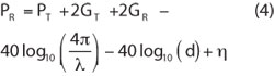
where PT is the power fed into the reader antenna, GT and GR is the gain of the interrogating reader antenna and CNT antenna sensor, respectively, and d is the distance between both. In Equation 4, except for the term η, all the values remain constant before and after the RFID tag meets the gas. Therefore, the variation of the backscattered power level solely depends on η, which is determined by the impedance of the SWCNT film in the CNT-based antenna sensor, as shown in Figure 11.
Graphene-Based WISP Wireless Gas Sensor
In addition to CNT materials, inkjet-printed graphene has also been investigated as a potential sensor material to improve the sensor selectivity (the ability to distinguish between different types of gases), response and recovery time. The sensing structure of this device comprised of layers of graphene film inkjet selectively deposited atop silver nano-particle-based feeding lines using a special inkjet printing technique/recipe on a robust Kapton substrate due to its robust tolerance to the harsh reduction environment required for extracting graphene. Figure 12 shows the final sensor that was integrated with the WISP platform to remotely sample, store and transmit the sensed information using the RFID EPC Gen 2 protocol.15
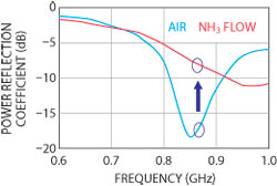
Figure 11 The calculated power reflection coefficient (η) of the CNT-based antenna sensor with a SWCNT film before and after the gas flow.
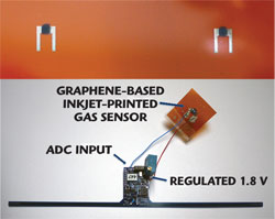
Figure 12 (a) Thin graphene films inkjet-printed in between and overlapping silver conductive inkjet-printed trace on Kapton substrate and (b) integrated WISP device.
The response time of the graphene sensor was tested by delivering a controlled concentration of ammonia gas in a semi-closed glass chamber to direct the flow of gas onto the sensor. The results of the measured resistance for 500 ppm of ammonia/air mixture are shown in Figure 13.20
Figure 13 DC resistance measurements of the graphene sample 1.
The graphene-based sensor demonstrates a fast response time, producing a resistance change of approximately five percent in response to the ammonia gas within three minutes. More interesting is the recovery time of the material. Within the first 15 seconds, the material is recovered by over 31 percent with no heating or UV treatments. Within the first minute, the material is recovered by over 80 percent. This result is different in comparison with the literature,21 where recovery times are generally on the order of several minutes. Additionally, the heating and UV treatments applied by some authors to achieve reported material recovery limits their usefulness in real-world environments.
Inkjet-Printed Ambient Wireless Power Scavenging Device
In addition to battery-less sensors and antennas, inkjet printing has also been successfully utilized to develop a wireless power scavenging platform that uses the ambient power currently found in the existing wireless spectrum to power up a wireless node (mote) made up of a microcontroller and a transceiver. Based on wireless spectrum measurements carried out in downtown Tokyo, a perpetual ambient source of wireless power was found in the frequency band from between 470 to 570 MHz, which is currently used for Analog (470 to 495 MHz) and Digital TV (520 to 570 MHz) broadcasts. These lower UHF bands offer superior propagation characteristics in terms of low attenuation through air and walls and also experiences lower parasitic losses through circuit components.
A review of microcontrollers and transceiver technology currently manufactured by a host of IC companies shows them to have the lowest operating voltage range of between 1.8 and 3.6 V. In order to completely eliminate the use of a battery, the wireless mote prototype was equipped with a low leakage super capacitor that was trickle charged with wireless power. Super capacitors have significant advantages over batteries through their significantly higher number of recharge cycles, low leakage, low cost and cleaner disposal. The drawback with capacitors is their unregulated voltage, which in the absence of proper supervision may discharge quickly, rendering the end device powerless. Lack of supervision of the charge-discharge mechanism of the capacitor into the end device may also cause it to undergo unnecessary power-on-resets (POR). In such a scenario, the MCU would turn on once the capacitor reached its turn on voltage drawing current from the capacitor, immediately causing the capacitor to discharge. Without sufficient voltage margin, the capacitor voltage would drop below the turn on voltage of the MCU, shutting it down before it can complete its firmware routine. With capacitors as power storage devices, there is always a risk of the MCU entering a state of constant PORs without finishing its functioning.
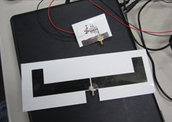
Figure 14 Inkjet-printed ambient wireless power scavenging device.
Preventing such a state has to be achieved through the proper design and calibration of the PMU circuit, which in essence is a voltage trigger analog switch that is set to a voltage sufficiently higher than the turn-on voltage of the MCU, but lower than the maximum operating voltage of the MCU along with proper firmware design. The operating time of the wireless mote would be the discharge time of the capacitor from the PMU triggered turn-on voltage to the turn off voltage of the MCU at 1.8 V.22
In order to ensure that the ambient wireless power in the UHF band (between 470 to 570 MHz) is transformed to the required voltage of 1.8 V and higher across the capacitor at a fixed distance from the power source, a topology comprising of a multistage RF voltage multiplier was used. RF Schottky diodes were used for the RF charge pumps given their lower forward voltage drop compared to conventional silicon-based PN diodes. Parasitic effects due to packaging currently limit the forward voltage of the diode to between 100 and 400 mV and forward currents of between 0.1 to 100 mA.22 This means any voltage received across the antenna terminals below this voltage would result in the antenna seeing an open impedance towards the circuit that would cause all the incident wireless power to be reflected back without turning on the device. In order to avoid this scenario at a given distance from the wireless source, a properly designed and laid out RF charge pump circuit was designed and optimally matched to the antenna to help transform and rectify the incident wireless power to a higher voltage, thereby ensuring a trickle charge into the end capacitor. The complete prototype capable of scavenging power from ambient TV signals at long ranges of over 6 km was fabricated using inkjet printing technology and is shown in Figure 14. The low turn on power of 35 μW in air is enough for the power scavenger to generate over 1.8 V at its output super capacitor. This is possible due to its low series dissipative losses (< 1.1 ohms)9,22 and almost exclusive charge pump capacitive reactance as shown by the input impedance of the power scavenger22 (see Figure 15). An output voltage of 1.8 V is capable of powering on most low power MCUs and wireless transceivers. Field measurements of the prototype carried out in Tokyo, Japan show the prototype capable of scavenging enough wireless power from a TV tower 6.5 km away.22
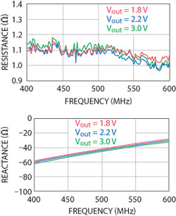
Figure 15 Input impedance of the ambient TV power scavenging device.
Conclusion
While batteries may be essential for reliable operation of applications requiring a more reliable and steadier supply, power scavenging techniques and zero-power nanostructure (e.g., CNT, graphene) based sensors can be reliably used for powering on a number of ubiquitous RFID and remote wireless sensing applications without the need for a battery, as shown in the prototypes presented in this article. By utilizing an optimized, selective metallization process such as inkjet printing, integrated 2D/3D battery-less power scavenging wireless sensing modules/motes operating at frequencies well into the UHF range and beyond can be successfully fabricated in an environmentally friendly and cost-effective way for numerous applications including Internet of Things, Smart Skins, Smart WSNs and wearable biomonitoring systems.
References
- V. Lakafosis, A. Rida, R. Vyas, Y. Li, S. Nikolaou and M.M. Tentzeris, "Progress Towards the First Wireless Sensor Networks Consisting of Inkjet-Printed, Paper-Based RFID-Enabled Sensor Tags," Proceedings of the IEEE, Vol. 98, No. 9, 2010, pp. 1601-1609.
- M. Lessard, L. Nifterik, M. Masse, J. Penneau and R. Grob, "Thermal Aging Study of Insulating Papers Used in Power Transformers," Electrical Insulation and Dielectric Phenomena 1996, IEEE Annual Report of the Conference, Vol. 2, 1996, pp. 854-859.
- L. Yang, A. Rida, R. Vyas and M.M. Tentzeris, "RFID Tag and RF Structures on a Paper Substrate Using Inkjet-Printing Technology," IEEE Transactions on Microwave Theory and Techniques, Vol. 55, No. 12, December 2007, pp. 2894-2901.
- A. Rida, L. Yang, R. Vyas, S. Basat, S. Bhattacharya and M.M. Tentzeris, "Novel Manufacturing Processes for Ultra-Low-Cost Paper-Based RFID Tags With Enhanced 'Wireless Intelligence'," Proceedings of the 57th IEEE-ECTC Symposium, Sparks, NY, June 2007, pp. 773-776.
- L. Yang and M.M. Tentzeris, "3D Multilayer Integration and Packaging on Organic/Paper Low-Cost Substrates for RF and Wireless Applications," ISSSE 2007 International Symposium on Signals, 2007, pp. 267-270.
- Cabot CCI-300 Conductive Nano-Silver Ink Datasheet, www.cabot-corp.com/New-Product-Development/Printed-Electronics/Products/Downloads/DL200811220115AM3822/
- J. Mujal, E. Ramon, E. Diaz, J. Carrabina, A. Calleja, R. Martinez and L. Teres, "Inkjet Printed Antennas for NFC Systems," Electronics, Circuits, and Systems (ICECS), 2010 17th IEEE International Conference, 2010, pp. 1220-1223.
- G. Shaker, S. Safavi-Naeini, N. Sangary and M.M. Tentzeris, "Inkjet Printing of Ultrawideband (UWB) Antennas on Paper-Based Substrates," IEEE Antennas and Wireless Propagation Letters, Vol. 10, 2011, pp. 111-113.
- R. Vyas, V. Lakafosis, M.M. Tentzeris, H. Nishimoto and Y. Kawahara, "A Battery-Less, Wireless Mote for Scavenging Wireless Power at UHF (470 to 570 MHz) Frequencies," IEEE Transactions on Antennas and Propagation (APSURSI), 2011, pp. 1069-1072.
- G. Shaker, M.M. Tentzeris and S. Safavi-Naeini, "Low-Cost Antennas for mm-Wave Sensing Applications using Inkjet Printing of Silver Nano-particles on Liquid Crystal Polymers," IEEE Transactions on Antennas and Propagation (APSURSI), 2011, pp. 1-4.
- G. Shaker, H.S. Lee, K. Duncan and M.M. Tentzeris, "Integrated Antenna with Inkjet-Printed Compact Artificial Magnetic Surface for UHF Applications," 2010 IEEE International Conference on Wireless Information Technology and Systems (ICWITS), 2010, pp. 1-4.
- S. Kim and M.M. Tentzeris, "Wearable Biomonitoring Monopole Antennas Using Inkjet Printed Electromagnetic Band Gap Structures," Proceedings of the 6th European Conference on Antennas and Propagation (EUCAP), 2012, accepted.
- R. Vyas, et al., "Paper-Based RFID-Enabled Wireless Platforms for Sensing Applications," IEEE Transactions on Microwave Theory and Techniques, Vol. 57, 2009, pp. 1370-1382.
- R. Vyas, A. Rida, L. Yang and M.M. Tentzeris, "Design, Integration and Characterization of a Novel Paper-Based Wireless Sensor Module," IEEE International Microwave Symposium, June 2008, pp. 1305-13078.
- "UHF Gen-2 System Overview," Texas Instruments, September 2005.
- J. Seybold, Introduction to RF Propagation, John Wiley & Sons, Hoboken, NJ, 2005, pp. 111-133, 163-179.
-
Lakafosis, X.H. Yi, T.R Le, E. Gebara,
Y. Wang and M.M. Tentzeris, "Wireless Sensing with Smart Skins," IEEE Sensors 2012. -
Z.Y. Lin, T.R. Le, J. Song, Y.G. Yao, Z. Li, K.S. Moon,
M.M. Tentzeris and C.P. Wong, "Preparation of Water-Based Carbon Nanotube Ink and its Application in Inkjet Printing of Carbon Nanotube Gas Sensor," Journal of Electronic Packaging, Vol. 98, No. 9, pp. 1601-1609, 2012. - R. Mangu, S. Rajaputra and V.P. Singh, "MWCNT-Polymer Composites as Highly Sensitive and Selective Room Temperature Gas Sensors," Nanotechnology, Issue 21, 2011.
- T. Le, V. Lakafosis, Z. Lin, M.M. Tentzeris and C.P. Wong, "Graphene-Based Inkjet-Printed WISP-Enabled Wireless Gas Sensor," submitted to IMS 2012.
- F. Schedin, et al., "Detection of Individual Gas Molecules Adsorbed on Graphene," Nature Materials, Vol. 6, 2007.
- R. Vyas, H. Nishimoto, M. Tentzeris, Y. Kawahara and T. Asami, "A Battery-Less, Wireless Mote for Scavenging Wireless Power at UHF (470 to 570 MHz) Frequencies," submitted to the IEEE International Microwave Symposium, 2012.
Manos M. Tentzeris received his degree in Electrical and Computer Engineering from the National Technical University of Athens (Magna Cum Laude) in Greece and MS and PhD degrees in Electrical Engineering and Computer Science from the University of Michigan, Ann Arbor, MI. He is currently a Professor with the School of ECE, Georgia Tech, Atlanta. He has published more than 420 papers in Journals and Conference Proceedings, five books and 19 book chapters. He is also an IEEE Fellow and IEEE MTT Distinguished Microwave Lecturer.
Rushi Vyas received his B.S. and M.S. degrees in Electrical Engineering from the Georgia Institute of Technology, Atlanta, in 2005 and 2010. He is currently a researcher at the ATHENA research group at the Georgia Institute of Technology while pursuing his PhD degree. He has authored/co-authored over 20 research works in peer-reviewed journals, conference proceedings and book chapters covering areas of antenna design, wireless and low power electronics, sensors, ubiquitous computing and energy harvesting. His work has been recognized in MSN News, Engadget and Design World.
Vasileios Lakafosis (S'07) received his Diploma degree in Electrical and Computer Engineering from the National Technical University, Athens, Greece, in 2006 and his M.Sc. degree in Electrical and Computer Engineering from the Georgia Institute of Technology, Atlanta, in 2009. He is currently pursuing his PhD degree at the Georgia Institute of Technology. Lakafosis has worked for Microsoft Research, the Cisco Research Center and the University of Tokyo. He has authored and co-authored two book chapters and over 15 papers in peer-reviewed journals and conference proceedings.
Taoran LE received her B.S. ('05) in Applied Physics from Hefei University of Technology. She received her M.S. degrees ('11) in Electronic Engineering from Politecnico di Torino in Italy and the Institut Polytechnique de Grenoble in France. She is currently a research assistant in the ATHENA group at Georgia Institute of Technology.
Amin Rida received his B.S., M.S. and Ph.D. degrees in Electrical and Computer Engineering from the Georgia Institute of Technology. He is currently a Systems Engineer at Northrop Grumman. He has authored and co-authored three books/chapter, seven journal papers, 30 conference papers in peer reviewed publications and has four pending patents.
Sangkil Kim received his bachelor's degree in Electrical and Electronic Engineering from Yonsei University, Seoul, Republic of Korea, in 2010. At present, he is pursuing his PhD degree at the Georgia Institute of Technology, Atlanta. He is now a research assistant at ATHENA group.