Rapidly growing wireless systems call for low loss filters with special requirements such as a suppressed second harmonic and a wide stop band region. Although conventional parallel coupled-line filters have many salient features,1 their spurious response at 2fo make them unsuitable for modern day wireless systems. This spurious response occurs because of the unequal even- and odd-mode phase velocities at 2fo. Various techniques have been reported to equalize the phase velocities at 2fo and thereby suppressing the spurious response.2–8 Using lumped capacitive loading, spurious suppression and miniaturization in parallel coupled-line filters have been reported.2 Some techniques3–6 use either stepped impedance resonators, wiggly-coupled-line resonators or mostly rely on choosing the proper dimensions for coupled-lines and substrate suspension heights for equalizing the phase velocities at 2fo. Spurious suppression in microstrip line filters has been obtained by using floating grounds.7 Using periodical non-uniform microstrip coupled-lines, spurious rejection has been achieved.8
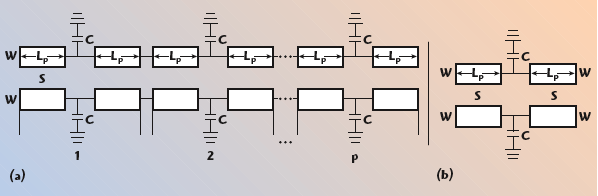
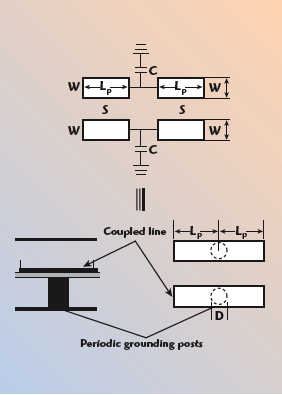
This article reports another technique that uses coupled-lines with periodically loading capacitances to suppress the second harmonic, 2fo. Periodic capacitive loading of a coupled-line section of an SSS filter is shown in Figure 1. Figure 2 shows a typical coupled-line section with ‘p’ periodical cells, each having a length of 2Lp and a capacitance placed at the center of the cell. The number of periodically loaded cells ‘p’ and the values of the capacitors C in each coupled-line section can be properly chosen to achieve the desired harmonic suppression. A circuit simulator such as Ansoft Designer 2.0 can be efficiently used to design filters by treating each periodic cell, as shown in the figure.
Design Procedure
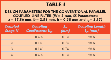
A bandpass filter at 2.4 GHz has been designed to demonstrate the validity of the proposed configuration with the following specifications: fo = 2.4 GHz, bandwidth = 15 percent, ripple = 0.1 dB and filter order N = 3. Based on the filter specifications, a standard synthesis procedure5 is used to calculate the required coupling coefficients. The corresponding physical dimensions are given in Table 1. The equivalent circuit of the periodic cell is used along with the synthesized coupled-line dimensions to obtain the required loading capacitance for the suppression of the second harmonic. Ansoft Designer 2.0 was used to simulate the filter shown in Figure 3 with N = 3 and p = 2.
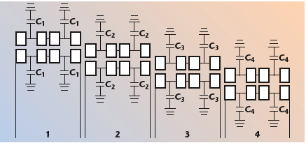
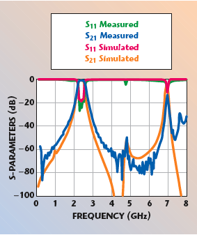
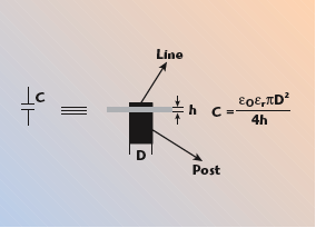
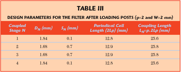
Due to the loading of the capacitances, the filter center frequency may be shifted. This can be corrected by reducing the length of the resonators. The capacitance value varies in each coupled-line section to obtain second harmonic suppression (for fixed ‘p,’ W and S). After achieving second harmonic suppression, the filter is fine-tuned to get the exact filter center frequency and bandwidth. Table 2 lists the required capacitances in each section. Each section utilizes two periodic cells. Finally, the required low values of lumped capacitances are realized by using circular posts, as shown in Figures 4 and 5. The posts’ dimensions are given in Table 3. To verify the accuracy of the design procedure, the method of moments-based planar EM simulator IE3D has been used to simulate the entire filter and the results are compared with the ones from the Ansoft Designer in Figure 6.
Conclusion
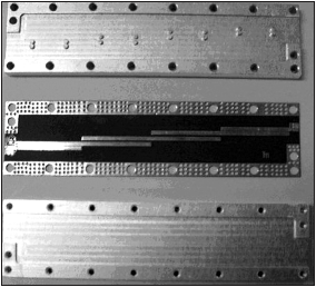
Figure 7 shows a photograph of the filter, which has periodically elevated posts in the bottom cavity to achieve the desired harmonic suppression. Figure 8 compares the measured results of the fabricated filter against the simulation results. A suppression level better than 50 dB can be observed. The return loss is better than 17 dB and the maximum insertion loss is 0.8 dB. The measured results compare well with the simulation results. This procedure, being simple to implement, offers relaxed dimensions for the coupled-lines and also improves the mechanical rigidity (due to the supporting posts) over conventional SSS filters.
References
1. G. Matthaei, L. Young and E.M.T. Jones, Microwave Filters, Impedance Matching Networks and Coupling Structures, Reprint Edition, Artech House Inc., Norwood, MA, 1985.
2. S.S. Myoung and J.G. Yook, “A Miniaturization Method of Parallel Coupled Line Filters Using Lumped Capacitors and Grounding,” Microwave Journal®, Vol. 48, No. 6, June 2005, pp. 94–100.
3. M. Makimoto and S. Yamashita, “Bandpass Filters Using Parallel Coupled Stripline Stepped Impedance Resonators,” IEEE Transactions on Microwave Theory and Techniques, Vol. 28, No. 12, December 1980, pp. 1413–1417.
4. L.G. Maloratsky, “Improve BPF Performance with Wiggly-coupled Lines,” Microwaves & RF, April 2004, pp. 54–62.
5. J.T. Kuo, M. Jiang and H.J. Chang, “Design of Parallel Coupled Microstrip Filters with Suppression of Spurious Resonances Using Substrate Suspension,” IEEE Transactions on Microwave Theory and Techniques, Vol. 52, No. 1, January 2004, pp. 83–89.
6. D. Packiaraj, M.Ramesh and A.T. Kalghatgi, “Second Harmonic Suppressed SSS Bandpass Filter,” Microwave and Optical Technology Letters, Vol. 48, No. 3, March 2006, pp. 600–602.
7. M. del Castillo Velazquez-Ahumada, J. Martel and F. Medina, “Parallel Coupled Microstrip Filters with Floating Grounding Plane Conductor for Spurious-band Suppression,” IEEE Transactions on Microwave Theory and Techniques, Vol. 53, No. 5, May 2005, pp. 1823–1828.
8. S. Sun and L. Zhu, “Periodically Nonuniform Coupled Microstrip-line Filters with Harmonic Suppression Using Transmission Zero Reallocation,” IEEE Transactions on Microwave Theory and Techniques, Vol. 53, No. 5, May 2005, pp. 1817–1822.
D. Packiaraj received his BE degree in electronics and communications engineering from Madurai Kamaraj University, Madurai, India, in 2000, and his ME degree in communications systems from Regional Engineering College, Trichirappalli, India, in 2002. He is currently a research staff member at the central research laboratory of Bharat Electronics Ltd., Bangalore, India. His areas of interest include filters, phase shifters and feed networks for antennas.

M. Ramesh received his BE degree in electronics and communications engineering from Andhra University, Viskhapatnam, India, in 1990, and his MTech degree in microwave engineering from the Indian Institute of Technology, Kharagpur, India, in 1993. He is currently a senior research staff member at the central research laboratory of Bharat Electronics Ltd., Bangalore, India. His research interests include microwave circuits and antennas.
A.T. Kalghatgi received his BE degree from Mysore University, India, in 1980, and his MTech degree in microwave and radar engineering from the Indian Institute of Technology, Kharagpur, India, in 1983. From 1983 to 1988, he was with the Avionic Design Bureau of Hindustan Aeronautics Ltd., Hyderabad, India. He obtained his PhD degree in microwave electronics from the University of Leeds, UK, in 1993. From 1988 to 1994, he was at the University of Leeds, first as a commonwealth scholar, then as a postdoctoral fellow. He is currently a principal scientist at the central research laboratory of Bharat Electronics Ltd., Bangalore, India. His professional interests include R&D of microwave and millimeter-wave systems, RF and microwave antennas, and secure and spread spectrum communication systems.