
High-Linearity Broadband LNAs
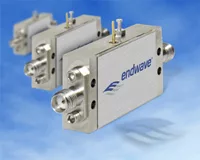
SAN JOSE, CA—July 30, 2008—Endwave Corporation (NASDAQ: ENWV), a provider of high-frequency RF modules for telecommunications networks, defense electronics and homeland security systems, has announced the release of three new high-linearity broadband low noise amplifiers which preserve signal purity by minimizing the non linear contributions. These amplifiers simultaneously achieve several high performance characteristics in a unique wideband design, and are available in three frequency bands of 0.5 to 2 GHz (JCA02-4000), 2 to 4 GHz (JCA24-4001), and 4 to 8 GHz (JCA48-4000).
They feature noise figures of under 2 dB up through C-Band, output P1dB levels of +24 dBm, and output IP3 headroom levels of 15 dB or greater above the output P1dB compression point. In addition, units deliver saturated output power levels approaching +27 dBm, have excellent I/O return loss of 11 dB min across the entire operating bandwidth, and provide signal gain of 35 dB or more. They deliver stable performance over a temperature range of -54º to + 85 ºC and draw just 425 mA of current from a standard 12 Volt supply. With the addition of a low drop out voltage regulator, customers may run these components on as little as 8 Volts DC for lower power dissipation applications.
These amplifiers are manufactured using stringent Design for Manufacturability (DFM) techniques, and are produced with high-precision automated assembly equipment to ensure repeatability. As such, they are often delivered in gain/phase matched sets, making them ideal for applications that require unit-to-unit repeatability such as phased array radar.
“We find that system designers are increasingly challenged to provide broadband performance without sacrificing key parameters such as noise figure, linearity, or return loss. Our amplifier design was created to simultaneously meet several of the design challenges with a single amplifier solution,” said Hung Nguyen, Sr. Design Engineer at Endwave. “Typical design challenges were overcome through careful selection of the transistor epi and gate peripheries, and a systematic analysis of non-linear contributions throughout the entire module component chain. We supplemented this approach by back-fitting with actual laboratory measurements of linearity and distortion to further improve our design.”
At the design stage, optimizing the impedance matching and bias of each of the active elements for top linearity, and carefully sequencing successively larger active elements, result in superior amplifier module performance.
The amplifiers are available with a variety of options including: variable gain control; I/O isolators, input limiters, limiting amplifiers, TTL switches, phase tracking, low phase noise, temperature compensation, detector outputs, and bias-T outputs. They are available in hermetic packages with a variety of connector options, including K, SMA, and GPO connectors.