
Modern mobile communication systems use band-limited linear modulation schemes, such as multi-level quadrature amplitude modulation (QAM) and quadrature phase shift keying (QPSK), which have high peak-to-average power ratio characteristics. For these systems, linear power amplifiers are needed to prevent adjacent channel interference.
A power amplifier operated sufficiently below the saturation level is a preferred method to solve the linearity problem. However, this results in a low efficiency power amplifier. Low efficiency means that most of the power is dissipated as heat and causes poor reliability. Moreover, it is very important to achieve high efficiency in order to minimize the amount of prime power needed and hence the cooling requirements, all of which translate into reduced cost.
Many solutions have been proposed to solve this problem. The Doherty amplifier is one of the most promising. It has the advantage of high efficiency and appropriate linearity even when the output power is far from the saturation point.
A Doherty amplifier consists of a carrier amplifier, a peak amplifier and a power combining network. A well-known embodiment of the combining network is suggested by R.J. McMorrow, et al.1 It is fabricated on a microstrip substrate and consists of two λ/4 transmission lines. However, when it comes to size, this configuration has some problems because of the relatively long length of a λ/4 transmission line.
This article presents a new type of power combining network, which consists of an arbitrary length of the transmission lines and shunt connected capacitors. The proposed structure is suitable for small size circuits because of the reduced length of the transmission lines.
Basic Principles of the Proposed Topology
The operation of a Doherty amplifier can be explained by load modulation.2 The output of the carrier amplifier after passing through an inverter is combined with the output of the peak amplifier, as shown in Figure 1.
 | ||
| Fig. 1 Schematic of a typical Doherty amplifier. | ||
The carrier amplifier operates in class B; the peak amplifier operates in class C. At this bias level, the peak amplifier operates at –6 dB below saturation. At low power, the carrier amplifier sees a 2Ropt load (Ropt is the optimum load impedance for a class B amplifier) and operates as a class B amplifier. The efficiency increases up to its maximum until it reaches a 6 dB level below the maximum power. As the input power increases to the medium power level, the peak amplifier becomes active. The current supplied by the peak amplifier decreases the load impedance of the carrier amplifier to Ropt. Active load pull can be achieved by changing the load impedance from 2Ropt to Ropt. At the maximum power level, both amplifiers see a load equal to Ropt and each amplifier provides half of the power to the system. The maximum efficiency is the same as the 78.5 percent of an ideal class B power amplifier. Load modulation is the key point in Doherty amplifier operation. The load modulation is realized by the reactive power combining structure with an impedance inverter.
Impedance Inverter
The impedance inverting network suggested by Doherty is a low pass filter with a 90° phase constant at the resonance frequency.3 Alternatively, it can be realized with quarter-wave transmission lines,1 as shown in Figure 2. The 50 Ω transmission line is an impedance inverter for load modulation. The 35.4 Ω quarter-wave transmission line is an impedance transformer for impedance matching between the amplifier and the external system. Even though this configuration is excellent and useful for various applications, it has some drawbacks regarding its large size because of the length of the λ/4 transmission lines.
 | ||
| Fig. 2 Conventional combiner fabricated with microstrip lines. | ||
Proposed power combining network for A doherty amplifier
The proposed structure is based on the fact that a quarter-wavelength impedance inverter can be replaced with an arbitrary length of transmission line and shunt capacitances, as shown in Figure 3.4
 | ||
| Fig. 3 Impedance inverter using (a) a quarter-wavelength line and (b) a line of arbitrary length and capacitors. | ||
The ABCD parameters of a λ/4 impedance inverter are given by
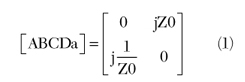
and the ABCD parameters of the impedance inverter with arbitrary line length are given by
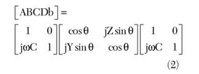
where
Z0 = line impedance of the λ/4 transmission line
C = shunt capacitor
Z = line impedance of arbitrary length line
θ = electrical angle of arbitrary length line
ω = angular frequency
Finally, from Equations 1 and 2, the elements of the arbitrary length line impedance inverter can be obtained using

Appendix A illustrates the design procedure for the proposed power combining network. The equivalent circuit of the conventional output network shown in (a) can be broken into two transmission lines and replaced by arbitrary electrical length line and four shunt capacitance, as shown in (b). The final configuration of the Doherty combining network is illustrated in (c). At the junction of the two transmission lines, the two shunt capacitors can be merged into a single one. This makes the final configuration more compact and reduces the cost.
Design and Experimental Results
The carrier and peak amplifiers were designed using Fujitsu’s FLL171ME GaAs FET. The carrier amplifier is operated in class AB mode (0.1Idss = 60 mA) and the peak amplifier is operated in deep class C mode (Vgs = –2.29 V). A reference class AB amplifier was also tested for comparison. Two identical transistors are used for both the reference and Doherty amplifiers.
Table 1 shows the shunt capacitances and characteristic impedances of the series transmission lines for the Korea PCS band (1830 to 1870 MHz). While any electrical length can be chosen for the new structure, λ/8 transmission lines were selected in this case. ATC’s 100A series capacitors are used for the shunt elements.
 | ||
Figure 4 is a photograph of the proposed combiner fabricated on a 30 mil thick Taconic RF35 substrate having a relative dielectric constant of 3.5. The size of the new combiner (14.4 x 16.0 mm) is relatively small compared with the conventional combiner using two λ/4 transmission lines (23.7 x 25.5 mm).
 | ||
| Fig. 4 The Doherty combining structures; (a) conventional and (b) reduced size. | ||
Figure 5 shows the experimental results obtained with a CW one-tone signal. The data for a class AB amplifier is also shown for reference. The gain of the Doherty amplifier is approximately 1.5 dB lower than the reference amplifier, although the efficiency is improved throughout the wide output power range, compared to the reference class AB amplifier.
 | ||
| Fig. 5 The amplifier’s properties measured at 1855 MHz. | ||
The spectrum mask of an IS-95 CDMA signal, which has a 10 dB peak to average power ratio (PAPR) is shown in Figure 6. At the output power level of 25.5 dBm the drain efficiency of the reference amplifier is 23.2 percent, while for the Doherty amplifier it is 35.8 percent. However, the adjacent channel power ratio (ACPR) of the Doherty amplifier is somewhat lower than for the reference design. This is due to the reduction in power capacity of the class C biased peak amplifier.
 | ||
| Fig. 6 IS-95 CDMA ACPR for the reference and Doherty amplifiers measured at 1855 MHz. | ||
Conclusion
A new type of power combining network for Doherty amplifiers has been presented. The proposed structure has series transmission lines of arbitrary length and shunt capacitors. In this article, a λ/8 transmission line length is chosen for the realization. The reduced size of this structure is useful for small size fabrications, such as microwave integrated circuits (MIC) and monolithic microwave integrated circuits (MMIC).
References
- R.J. McMorrow, D.M. Upton and P.R. Maloney, “The Microwave Doherty Amplifier,” IEEE 1994 International Microwave Symposium Digest, Vol. 3, pp. 1653–1656.
- S.C. Cripps, RF Power Amplifiers for Wireless Communication, Artech House Inc., Norwood, MA, 1999, pp. 225–235.
- W.H. Doherty, “A New High Efficiency Power Amplifier for Modulated Waves,” Proceedings of the IRE, Vol. 24, No. 9, 1936, pp. 1163–1182.
- T. Hirota, A. Minakawa and M. Muraguchi, “Reduced-size Branch-line and Rat-race Hybrids for Uniplanar MMICs,” IEEE Transactions on Microwave Theory and Techniques, Vol. 30, No. 3, March 1990, pp. 270–275.
Hyeong Tae Jeong received his BSEE and MSEE degrees from Sogang University, Seoul, South Korea, in 1995 and 1997, respectively. From 1997 to 2002, he worked as a senior engineer for Samsung Electronics. He is currently working toward his PhD degree. His research interests include linearization and efficiency enhancements of RF power amplifiers.
Chul Dong Kim received his BS degree in electronic engineering from Seoul National University, Seoul, South Korea, in 1971, and his PhD degree in electronic engineering from the University of Wisconsin in 1985. He is the president and CEO of Sewon Teletech Inc., a company that specializes in RF power amplifiers.
Chul Dong Kim received his BS degree in electronic engineering from Seoul National University, Seoul, South Korea, in 1971, and his PhD degree in electronic engineering from the University of Wisconsin in 1985. He is the president and CEO of Sewon Teletech Inc., a company that specializes in RF power amplifiers.
