

With the ever-increasing complexity in today’s high frequency and high speed circuit designs, designers appreciate the development time and cost savings that can come from accounting for electromagnetic (EM) effects up-front in designs. However, many designers still see EM point tools as an expensive luxury that is best left to EM gurus who exercise high end software to its fullest. What if practical, EM accuracy could be had for a fraction of the typical cost? What if EM simulation could be as common and accessible as circuit simulation?
The new Electromagnetic Design System (EMDS) 2006A (see Figure 1), from Agilent Technologies’ EEsof EDA division, seeks to fill this price performance gap, making full 3D EM simulation an attractive and economical option for designers working with RF circuits, MMICs, PC boards, modules and signal integrity applications. The software package provides the best price performance 3D EM simulator on the market, with a full 3D electromagnetic field solver, a modern solid modeling front-end, and fully automated meshing and convergence capabilities for modeling arbitrary 3D shapes such as connectors, machined parts, components, bond wires, antennas and packages.
Based on Industry-proven Finite Element Method Simulation Technology
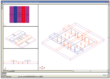
The finite element method (FEM) divides the full problem space into smaller regions and represents the field in each sub-region, or element, with a local function. In EMDS, the geometric model is automatically divided into a number of tetrahedra, where a single tetrahedron is formed by four triangles. This collection of tetrahedra is referred to as the finite element mesh. Figure 2 shows the finite element mesh that was created for a sample structure. The finite element mesh is an efficient and accurate way to divide and solve for EM effects in a wide variety of high frequency 3D geometries.
The finite element mesh can be tuned to meet the accuracy standards of the designer. The finer the mesh, the more accurate the 3D EM solution. The tradeoff is in simulation time. The designer has control over the fine-ness of the mesh.
EM Design System Features
EMDS features include:

-
Arbitrarily shaped 3D passive structures for generalized EM analysis
-
Conductors, resistors, isotropic and anisotropic dielectrics, isotropic and anisotropic linear magnetic material modeling allow a wide range of application coverage
-
An unlimited number of ports, which enables simulating multi-I/O design applications such as packages
-
Electric and magnetic fields modeling, allowing visualization of EM fields in a design
-
Absorbing boundary condition (free space), allowing antenna modeling
-
Full-wave, EM-accuracy for first-pass design success
-
Multi-mode impedance and propagation constants that overcome single-mode modeling limitations in many other EM modeling tools
-
Antenna parameters (gain, directivity, polarization and so on), to allow better insight into antenna design
-
An EMDS/ADS link, providing an integrated approach to EM/circuit design
Integration with Leading RF and Microwave Design Flow Versus Expensive Point Tools
Today’s 3D EM modeling experts have been required to invest heavily in sophisticated 3D EM point tools that allow them to study the EM behavior of complex high frequency/ high speed designs. However, these “experts” are few and far between. When the cost and complexity of 3D EM point tools prohibit their use, RF and microwave engineers may choose not to study EM effects. They may instead revert to rule-of-thumb methods and guesses to push a design forward, in hopes that the design will work after a few tries.
With Agilent’s popular 3D planar tool, Momentum, fully integrated into the company’s Advanced Design System (ADS), the new Electromagnetic Design System gives RF and microwave engineers access to the most comprehensive EM simulation tools in the industry-leading RF/microwave design flow. Agilent’s circuit and system design tools include both the ADS EDA platform and the GENESYS RF and microwave design software. The EMDS roadmap includes increasingly tight integration with both ADS and GENESYS.
Used to Design Cutting Edge Products
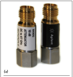
Behind every EDA design tool is the accumulated knowledge and expertise of the people who not only build the software, but of those who use it and put it through its paces. Agilent is unique in the marketplace as an EDA company inside a test and measurement organization, actually using these EDA tools to design virtually all of the company’s RF and microwave instruments and related products. For example, the technology in EMDS was recently used to design the company’s 8490G precision coaxial fixed attenuators. These attenuators are used to maximize their users’ operating frequency range up to 67 GHz with industry-leading attenuation accuracy, coupled with low SWR and a variety of attenuation options to suit users’ application needs. Figure 3 shows these precision attenuators and a solid model representation of the attenuators in EMDS.
Conclusion
The new Electromagnetic Design System occupies an important price performance niche for RF/microwave circuit designers. Its addition makes 3D EM simulation an attractive and economical option for designers who need to account for EM effects in today’s increasingly high frequency and high speed designs. The simulation package offers full 3D EM modeling capabilities with integration into Agilent’s industry-leading RF/microwave circuit design flow. It is a new tool that lowers the economic barrier and will find a way to desktops throughout the RF/microwave design community.
Agilent EMDS 2006A is expected to ship in July 2006, with prices starting at approximately $15K. For more information about EMDS and Agilent’s other EDA offerings, visit www.agilent.com/find/eesof.
Agilent EEsof EDA,
Santa Rosa, CA (800) 829-4444,
www.agilent.com