
The addition of a small amount of C in the B-doped base layer of a npn SiGe heterojunction bipolar transistor (HBT) paved the way for exposing the high frequency (HF) performance potential of such devices more than 10 years ago.1 Significantly, the suppression of thermal diffusion and point-defect assisted enhanced diffusion, due to the presence of C, helps to sustain steep base profiles through the fabrication process. As a consequence, the base transit time, the crucial delay time in previous HF bipolar transistor generations, could be reduced without degradation of the base sheet resistance, by realizing a highly-concentrated, narrow base doping in combination with a carefully tailored SiGe profile.
A further substantial decrease of the total transit time, τEC, or the transit frequency, fT =1/(2πτEC), can be achieved only if the emitter and collector resistances, as well as the charging times of the base-emitter and base-collector space-charge regions, are reduced adequately. The introduction of a mono-crystalline emitter2 and the vertical scaling of the emitter-base and base-collector junction contributed to the fT progress.
However, specifying fT alone is not sufficient to characterize the high speed performance. Another important figure of merit, in evaluating the HF behavior, is the maximum oscillation frequency, fmax. The base resistance, RB, the base-collector capacitance, CBC, and fT are associated with fmax by the expression fmax = √ (fT/(8πRBCBC)). On one side, fmax can be increased by optimizing the vertical profile with respect to fT and the internal components of RB and CBC. On the other side, fmax can be improved if the parasitic effects that are particularly caused by the external contributions of RB and CBC are decreased. In reality, both situations have to be considered simultaneously, because device architecture, process flow, lateral dimensions and reliability constraints influence each key parameter.
These efforts to achieve optimization resulted in SiGe HBT performance improvements from a fT/fmax level of approximately 50 to 100 GHz to values of 200 to 300 GHz during the course of 10 years, starting from the mid-1990s. The integration of best SiGe bipolar performance into CMOS technologies down to the 0.13 μm node3-5 and the superior HF analog capabilities of the bipolar versus CMOS devices6 enabled the penetration of SiGe HBTs into the communication market.7 Upcoming new applications in the fields of THz imaging and sensing, or high speed/high bandwidth communications at even higher frequencies, raise the question as to what extent the SiGe HBT or BiCMOS technologies could occupy this area, especially since further scaled, pure CMOS technologies are hardly able to meet these needs.
Recently, the three-and-a-half-year European DOTFIVE8 project addressed the task of pushing the HF performance limits of SiGe HBTs. From February 2008 to July 2011, a consortium of 15 partners from industry and academia focused on the demonstration of a half Terahertz fmax SiGe HBT or a ring-oscillator gate-delay of 2.5 ps. A detailed summary was produced.9
In the project, IHP took two different approaches. The first, not presented here, intends to overcome scaling issues of the classical double-polysilicon (DP) technology that is widely used in industry.4,10 This device architecture utilizes a selective epitaxial growth (SEG) of the base layer. The emitter window is self-aligned, not only to the external base region, but also to the internal collector region. It is clear that a selectively implanted collector (SIC) can also be formed, that is easily self-aligned to the emitter window. Promising results for a SEG DP technology with an unconventional way to form the external base were achieved.11
A second SiGe HBT approach, that is explained in this article, comprises the non-selective epitaxial growth (NSEG) of the SiGe base layer, completed by a self-aligned (SA) arrangement of the emitter window and the highly-doped, elevated external base region. The basic HBT process flow has been presented.12 The HBT development of this work is performed in IHP's 0.25 μm SG25H1 BiCMOS technology.13
Progress in the performance of this established NSEG concept was realized during the course of the project,14 step by step, by introducing a set of process modifications. Starting from the initial DOTFIVE generation D51, this article describes technological changes implemented in the final D53 version and their implications on the HF parameters. Based on this development, fT/fmax values of 300 GHz/500 GHz and a CML ring-oscillator gate delay of 2.0 ps were reached.
HBT Module Fabrication
The HBT module is fabricated in IHP's 0.25 μm SG25H1 BiCMOS technology environment. For this purpose, one poly-resistor, 5 Al metal layers and a 1 fF/μm2 MIM capacitor are used. The process flow starts with the formation of the shallow-trench isolation (STI), the deep n well layer for the vertical isolation of nMOSFETs, the CMOS wells and gates, including gate spacer etching. Before HBT fabrication, the wafer is covered with a layer stack protecting the CMOS regions (Figure 1a). Then, the highly-doped collector well is formed. A resist mask is patterned to open the HBT regions (first lithography step M1), followed by the well implantation (Figure 1b) and anneal. The deep-trench (DT) free collector wells15 are not deeper than the STI. Consequently, the active transistor and the collector contact region is not separated by STI to ensure a low collector resistance, RC, and a low collector-substrate capacitance, CCS. An additional advantage of this collector design, dedicated to achieve the highest HBT speed, is the possibility of obtaining collector profiles on the base side, which are steeper than those of the conventional buried-layer process, due to a reduced thermal treatment. Moreover, the thermal resistance associated with the DT-free architecture is reduced.
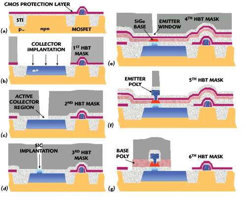
Figure 1 Schematic cross sections at different steps of the device fabrication.
After forming the highly-doped collector, the NSEG HBT module is subjected to the deposition and structuring of an oxide layer to define the active collector region (M2 in Figure 1c). The resulting windows in the oxide layer then have to be filled with silicon. At this point, an essential process change was introduced in the course of the project. In the final process generation D53, after filling the gap in the oxide layer by selective epitaxy, the SIC is formed with the help of a patterned resist mask before non-selective base deposition (M3 in Figure 1d).
Subsequently, the base layer is grown at a later stage. In previous generations, only one epitaxial step was carried out, while the SIC was arranged after base epitaxy, simultaneously with the emitter-window opening. Although this modification means greater effort and gives up the self-alignment of the SIC to the emitter window, it improves the possibility of tailoring the low-doped collector profile as the degradation of the base profile is avoided, together with an improvement in the HF performance.
At this point, a further modification has to be mentioned, which affects the design of the external base-collector region. The best HF results are achieved for a crystal orientation of the wafer substrate which is rotated by 45° compared to the standard configuration. The primary reason for this effect is attributed to the suppressed growth of facets along side-walls of dielectric layers during selective epitaxy.
Compared to the initial process generation D51, the B-doped SiGe base profile is optimized. The Ge content and the B dose are increased in such a way that the collector current density is not decreased while the base sheet resistance is lowered. Essential features of the emitter-base architecture applied correspond to the process flow.12 These include deposition and patterning of an oxide/nitride/oxide layer stack to form the emitter window (M4 in Figure 1e), fabrication of emitter-base inside spacers, emitter formation, including deposition of a dielectric layer stack, emitter-polysilicon structuring (M5 in Figure 1f), elevating the external-base region by selective epitaxy, and finally patterning of the base polysilicon (M6 in Figure 1g).
A substantial reduction of the emitter-base oxide spacer width from 45 to 30 nm could be achieved by fine-tuning the combination of wet and dry etching applied to form the emitter-window inside-spacers. The lateral scaling also impacts on the minimum emitter window size that is reduced from 180 to 120 nm. Furthermore, the dimensions of the collector window and the emitter contact region are reduced by approximately 30 percent. Other advantages of increasing the HF performance include higher emitter doping, a lower sheet resistance of the silicide layer and the reduced temperature of the final spike anneal.
Device Results
Let's compare the electrical results for the initial DOTFIVE HBT generation D51 and the final generation D53 with NSEG. Gummel and output characteristics are shown in Figures 2 and 3. In these graphs, the current values are normalized to the effective emitter area, AE,eff, to give a better overview of the impact of process modifications. The measurements are performed at VCB =0 V and T = 300 K, on 8-emitter devices AE,eff = 8× (0.18 × 0.92) μm2 for D51 and AE,eff = 8 × (0.12 × 0.96) μm2 for D53.

Figure 2 Gummel plots of 8-emitter devices, normalized to the effective emitter area AE,eff for the HBT generations D51 and D53.

Figure 3 Output characteristics of 8-emitter devices, normalized to the effective emitter area AE,eff for the HBT generations D51 and D53.
As indicated in the Gummel plot, the collector current density is slightly increased in the final generation (6 percent at VBE = 0.7 V) despite a reduction of the pinched base sheet resistance, RSBi, from 3.5 to 2.6 kΩ. This result is not only due to the effective increase of the Ge content, but it is also influenced by the decrease of the spike anneal temperature and by moving the SIC implantation from afTer the base epitaxy to before it.
A higher Ge content also tends to produce higher base currents, IB, due to an increased neutral base recombination, whereas the elimination of SIC implantation through the base lowers IB. In addition, higher emitter doping increases IB markedly, due to an enhanced Auger recombination. Altogether, the base current density is enhanced only by 16 percent for the D53 versus D51.
Consequently, the peak current gain is very similar for both generations with values of approximately 700. In the output characteristics, it can be seen that the collector-emitter breakdown-voltage, BVCEo, is reduced from 1.7 to 1.6 V going from D51 to D53, which is attributed to the increased doping concentration of the SIC. Compared to a typical BVCEo of the 200 to 300 GHz SiGe HBT version, there is no deterioration. However, the SIC doping is not sufficient to prevent the increased collector resistance of D53 caused by the smaller collector window size (shown in Figure 3).

Figure 4 Transit frequency ƒT and maximum oscillation frequency ƒmax vs. collector current density normalized to AE,eff for the HBT generations D51 and D53.
In Figure 4, the transit frequency, fT, and maximum oscillation frequency, fmax, are plotted versus the collector current density, jC, which is referred to as AE,eff, with the same 8-emitter transistors being used for the DC measurements. To extract the fT and fmax, S-parameters were measured on wafer up to 110 GHz (network analyzer 8510 XF). The fT, fmax values are extrapolated at 40 GHz from the small-signal current gain h21 and the unilateral gain U respectively, with -20 dB per frequency decade, at VCE = 1.5 V and T = 300 K.
The sum of the base and the emitter resistances (RB+RE) is determined from the circle fit of S11 for a device operating at peak fT. In addition, the DC fly-back method is applied to specify RE. Although there is still no well-established procedure for extracting these parameters, it is assumed that the values presented in this article enable evaluation of the trend quantitatively.

Due to the variety of process modifications, a substantial improvement of fT/fmax is demonstrated for the D53 HBT generation with peak values of 300 GHz/500 GHz. The device parameters, shown in Table 1, indicate a 27 percent increase of fT and a 16 percent decrease of the normalized CBC for D53 compared to D51. However, the crucial contribution for improving fmax is originated by an approximate 50 percent reduction of RB for this HBT module in the DOTFIVE run time.
Comparing both HBT generations, the fT and fmax decay and, therefore, the onset of the Kirk effect is shifTed towards higher current densities in the final generation. Furthermore, jC at peak fT is increased from 13.5 mA/μm2 for D51 to 18.5 mA/μm2 for D53. The enhanced doping concentration of the SIC is responsible for this effect. The new base profile with higher Ge content and lower RSBi, combined with a lower final spike anneal, affects RB and fT positively.
Besides the reduced spike-anneal temperature (D51: 1,100° C > D53: 1,050°C), moving the SIC formation from afTer to before base deposition has contributed essentially to further improve RB and fT and consequently fmax. From the device parameters, it is estimated that the primary contribution of the improvement in fmax (approximately 70 percent) is due to structural process modifications, while the remaining 30 percent can be attributed to device scaling.14

Figure 5 CML ring oscillator gate delaty τ vs. current per gate normalized to AE,eff for oscillators consisting of 53 stages with single emitter HBTs fabricated in generation D51 and D53.
The CML ring oscillator (RO) has proven to be a powerful tool for evaluating the HF-performance progress of SiGe HBTs, because their gate delay shows a strong correlation to key parameters such as fT and fmax and because it delivers fast and reliable measured values. Now the gate delays of ROs will be compared using a single-ended configuration. The minimum gate delay τmin is decreased from 3.1 ps (D51) to 2.0 ps (D53) for a voltage swing ΔV of 300 mV at a supply voltage of VEE = -2.5 V (Figure 5). The supply voltage can be lowered to 1.7 V without affecting τmin if ΔV is reduced to 200 mV (Figure 6).
In the DOTFIVE project, not only CML ring oscillators were used to benchmark the performance of this NSEG HBT module – designers at the University of Wuppertal realized complex circuits in several DOTFIVE generations, representing new levels of high frequency circuit performance with respect to complexity.16

Figure 6 Minimum CML ring oscillator gate delay τ vs VEE.
Summary
Substantial progress with regard to the high speed performance of SiGe HBTs has been demonstrated, achieving the target of the European DOTFIVE project. The performance improvement of the HBT module, with non-selective base epitaxy and self-aligned emitter base architecture, is primarily based on modifications of the base profile, the wafer orientation, the annealing regime, the salicide sheet resistance, the emitter deposition and the selectively implanted collector. Approximately 30 percent of the fmax advance is due to lateral scaling of key HBT dimensions. Starting from the reference status, the process changes described in this article have led to peak fmax values of 500 GHz and minimum CML ring oscillator gate delays of 2.0 ps.
In collaboration with DOTFIVE partners, the new generation HBT has been tested successfully in complex circuits. This performance demonstrates the potential of SiGe HBTs for arising applications, such as sub-mm-wave imaging. Currently, work is being undertaken on the transfer of such performance levels into the 0.13 μm BiCMOS platform. This activity is facilitated by the fact that the fundamental HBT integration scheme of the standard 0.13 mm BiCMOS process is similar to the D53 module.
References
- H.J. Osten, G. Lippert, D. Knoll, R. Barth, B. Heinemann, H. Rucker and P. Schley, "The Effect of CaRBon Incorporation on SiGe Heterobipolar Transistor Performance and Process Margin," Technical Digest of the 1997 IEEE International Electron Device Meeting, pp. 803-806.
- S. Jouan, R. Planche, H. Baudry, P. Ribot, J. A. Chroboczek, D. Dutarte, D. Gloria, M. Laurens, P. Llinares, M. Marty, A. Monroy, C. Morin, R. Pantel, A. Perrotin, J. de Pontcharra, J.L. Regolini, G. Vincent and A. Chantre, "A High-speed Low 1/f Noise in SiGe HBT Technology Using Epitaxially-aligned Polysilicon Emitters," IEEE Transactions on Electron Devices, Vol. 46, No. 7, July 1999, pp. 1525-1530.
- B.A. Orner, Q.Z. Liu, B. Rainey, A. Stricker, P. Geiss, P. Gray, M. Zierak, M. Gordon, D. Collins, V. Ramachandran, W. Hodge, C. Willets, A. Joseph, J. Dunn, J.S. Rieh, S.J. Jeng, E. Eld, G. Freeman and D. Ahlgren, "A 0.13 μm BiCMOS Technology Featuring a 200/280 GHz (fT/fmax) SiGe HBT," Proceedings of the 2003 IEEE Bipolar/BiCMOS Circuits and Technology Meeting, pp. 203-206.
- G. Avenier, P. Chevalier, G. Troillard, B. Vandelle, F. Brossard, L. Depoyan, M. Buczko1, S. Boret, S. Montusclat, A. Margain, S. Pruvost, S.T. Nicolson, K.H.K. Yau, D. Gloria, D. Dutartre, S.P. Voinigescu and A. Chantre, "0.13 μm SiGe BiCMOS Technology for Mm-wave Applications," Proceedings of the 2008 IEEE Bipolar/BiCMOS Circuits and Technology Meeting, pp. 89–92.
- H. Rücker, B. Heinemann, W. Winkler, R. Barth, J. Borngrdöber, J. Drews, G.G. Fischer, A. Fox, T. Grabolla, U. Haak, D. Knoll, F. Korndörfer, A. Mai, S. Marschmeyer, P. Schley, D. Schmidt, J. Schmidt, K. Schulz, B. Tillack, D. Wolansky and Y. Yamamoto, "A 0.13 μm SiGe BiCMOS Technology Featuring fT/fmax of 240/300 GHz and Gate Delays Below 3 ps," Proceedings of the 2009 IEEE Bipolar/BiCMOS Circuits and Technology Meeting, pp. 166-169.
- P. Garcia, A. Chantre, S. Pruvost, P. Chevalier, S.T. Nicolson, D. Roy, S.P. Voinigescu and C. Garnier, "Will BiCMOS Stay Competitive for mmW Applications?" Proceedings of the 2008 IEEE Custom Integrated Circuits Conference, pp. 387-394.
- A.J. Joseph, "SiGe BiCMOS Technologies – Addressing the Communication Market Needs," 2004 IEEE Compound Semiconductor Integrated Circuit Symposium Digest, pp. 35-38.
- DOTFIVE available at www.dotfive.eu
- P. Chevalier, T.F. Meister, B. Heinemann, S. Van Huylenbroeck, W. Liebl, A. Fox, A. Sibaja-Hernandez and A. Chantre, "Towards THz SiGe HBTs," Proceedings of the 2011 IEEE Bipolar/BiCMOS Circuits and Technology Meeting, in press.
- J. Böck, H. Schäfer, K. Aufinger, R. Stengl, S. Boguth, R. Schreiter, M. Rest, H. Knapp, M. Wurzer, W. Perndl, T. Böttner and T.F. Meister, "SiGe Bipolar Technology for Automotive Radar Applications," Proceedings of the 2004 IEEE Bipolar/BiCMOS Circuits and Technology Meeting, pp. 84-87.
- A. Fox, B. Heinemann, R. Barth, S. Marschmeyer, Ch. Wipf and Y. Yamamoto "SiGe:C HBT Architecture with Epitaxial External Base," Proceedings of the 2011 IEEE Bipolar/BiCMOS Circuits and Technology Meeting, in press.
- H. Rücker, B. Heinemann, R. Barth, D. Bolze, J. Drews, U. Haak, W. Höppner, D. Knoll, K. Köpke, S. Marschmeyer, H.H. Richter, P. Schley, D. Schmidt, R. Scholz, B. Tillack, W. Winkler, H.E. Wulf and Y. Yamamoto, "SiGe:C BiCMOS Technology with 3.6 ps Gate Delay," 2003 IEEE International Electron Device Meeting Technical Digest, pp. 531-534.
- B. Heinemann, R. Barth, D. Knoll, H. R¸cker, B. Tillack and W. Winkler, "High-performance BiCMOS Technologies Without Epitaxially-buried Subcollectors and Deep Trenches," Semiconductor Science and Technology, Vol. 22, No. 1, January 2007, pp. 153-157.
- B. Heinemann, R. Barth, D. Bolze, J. Drews, G.G. Fischer, A. Fox, O. Fursenko, T. Grabolla, U. Haak, D. Knoll, R. Kurps, M. Lisker, S. Marschmeyer, H. R¸cker, D. Schmidt, J. Schmidt, M.A. Schubert, B. Tillack, C. Wipf, D. Wolansky and Y. Yamamoto, "SiGe HBT Technology with fT/fmax of 300 GHz/500 GHz and 2.0 ps CML Gate Delay," Technical Digest of the 2010 IEEE International Electron Device Meeting, pp. 688-691.
- B. Heinemann, H. Rücker, R. Barth, J. Bauer, D. Bolze, E. Bugiel, J. Drews, K.E. Ehwald, T. Grabolla, U. Haak, W. Höppner, D. Knoll, D. Krüger, B. Kuck, R. Kurps, M. Marschmeyer, H.H. Richter, P. Schley, D. Schmidt, R. Scholz, B. Tillack, W. Winkler, D. Wolansky, H.E. Wulf, Y. Yamamoto and P. Zaumseil, "Novel Collector Design for High-speed SiGe:C HBTs," Technical Digest of the 2002 IEEE International Electron Device Meeting, pp. 775-778.
- E. Öjefors, J. Grzyb, Y. Zhao, B. Heinemann, B. Tillack, U.R Pfeiffer, "A 820 GHz SiGe Chipset for Terahertz Active Imaging Applications," 2011 International Solid-State Circuits Conference Digest, pp. 224-226.
Bernd Heinemann received his master's degree in physics from the Humboldt University, Berlin, Germany, in 1984, and his doctorate in electrical engineering from the Technische Universität, Berlin, Germany, in 1997. He joined IHP in Frankfurt, Germany in 1984. His research activities include the development and characterization of MOS and bipolar devices and since 1993 he has been a member of a team working on the exploration and technological implementation of SiGe HBTs.
Alexander Fox received his diploma in electrical engineering from the RWTH Technical University, Aachen, Germany, in 1999, and his doctorate in engineering sciences from the Christian-Albrechts-Universität, Kiel, Germany, in 2006. In 2000, he joined IHP in Frankfurt, Germany, as a Research Assistant in the Process Integration Group, where he has been working on general integration issues of 0.25m BiCMOS technology, the integration of an embedded flash memory module into a SiGe:C BiCMOS baseline technology and SiGe bipolar transistors.