
The term electromagnetic compatibility (EMC) often conjures up images of FCC test labs, computing and/or wireless devices. However, in the automotive industry, the unintentional creation and reception of electromagnetic fields, a definition of electromagnetic interference (EMI), is becoming an ever greater concern. As automobiles become mobile hotspots and as the electronic content (wireless links, multi-media devices, electronic control modules, electric hybrid drives, etc.) of automobiles continues to increase, the control of and design for EMI and EMC become ever more important.
As a result of this rapid electrification of automobiles, a number of applicable standards have come into existence. One of the earliest of the industry directives was issued in Europe in 1972 as Automotive Directive 72/245/EEC. This directive was created to deal with the electronic spark plug noise. Since that time, the International Standards Organization, the Society of Automotive Engineers, and CISPR have created a variety of standards specifically for the automotive industry.
These standards are designed to ensure that all on-board systems continue to function properly during exposure to EMI or automatically return back to normal operating conditions after exposure or by a manual reset operation. A major concern for automotive EMI engineers is that a car can contain as much as five kilometers of wires. While cabling is an obvious source of EMI in a car, there are a number of other sources, especially in modern cars, which are packed with electronic devices. Lastly, it is important to note that drivers also introduce potential EMI sources in the form of cell phones or smart phones, tablets and other Bluetooth-enabled devices.
For the above reasons, conventional EMI/EMC procedures and techniques may not be appropriate for these new components and electronic devices. To address this, there are a few automotive standards trying to reduce the probability of EMI occurring in vehicles by making use of one of several laboratory tests. One of the most important of these standards is ISO 11451-2. This standard specifies that the electical performance of all electronic subsystems remains unaffected by electromagnetic disturbances that are generated by a source antenna, radiating the vehicle-under-test inside an anechoic chamber.
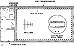
Figure 1a ISO 11451-2 test setup.
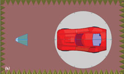
Figure 1b HFSS virtual test chamber.
The international standard ISO 11451-2 applies to road vehicles and is meant to determine the immunity of private and commercial vehicles to electrical disturbances from off-vehicle radiation sources, regardless of the vehicle propulsion system, including hybrid electric vehicles (HEV). The test procedure prescribes that the test be performed on a full vehicle in an absorber-lined shielded enclosure, which is meant to create a test environment that simulates open field testing. For this test, it is typical that the floor is not covered with absorbing material, but such covering is allowed. An example of a rectangular shielded enclosure is shown in Figure 1a. Figure 1b shows a virtual test chamber as modeled in a 3D electromagnetic simulation software package (i.e. HFSS™).
Testing for the ISO 11451-2 standard consists of generating radiated electromagnetic fields using a source antenna with radio frequency (RF) sources capable of producing the desired field strengths ranging from 25 V/m to 100 V/m and beyond. The test covers the range of frequencies from 10 kHz up to 18 GHz. During the test, all embedded electronic equipment must perform flawlessly. This flawless performance also applies to the frequency sweep of the source antenna.

Figure 2 Comparison of FEM, IE and FEBI models.
Performing the ISO 11451-2 standard test can be a very time consuming process, requiring expensive equipment and access to a very expensive test facility. Hence, numerical simulation can be a cost-effective means to reduce the design cycle of the product as well as its associated R&D costs. Full vehicle Finite Element Method (FEM) simulation has become possible within the past few years by using the domain decomposition method (DDM) that was pioneered by and available within the ANSYS® HFSS product. The DDM process parallelizes the entire simulation domain by creating a number of sub-domains, each of which are solved on different computing cores or various computers connected to a network. While the DDM procedure allows engineers to simulate entire vehicles, recent developments in simulation technology offer a superior approach to solving large electromagnetic structures. The technique is called the hybrid Finite Element Boundary Integral (FE-BI) methodology and has been made available in the ANSYS HFSS product within the last year (featured as a technical article in the January 2011 issue of Microwave Journal).
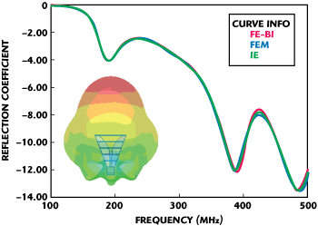
Figure 3 Comparison of validated far-field behavior using three different methods.
FE-BI is a numerical method that uses an Integral Equation (IE) based solution as a truncation boundary for the FEM problem space. This combination of solution paradigms allows users to dramatically reduce the solution volume that needs to be solved by the FEM method, resulting in a faster and more efficient simulation approach. Figure 2 shows how FE-BI can be used to reduce the solution volume required by a simulation. It is important to note that the distance from radiator to FE-BI boundary can be arbitrarily small and is often less than lambda by 10. This reduced solution space then leads to a decrease in the simulation time and reduces the overall computational effort.
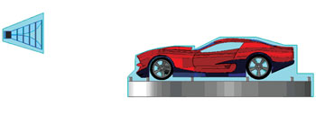
Figure 4 Two sub-regions used to simultaneously solve using FE-BI solver.
In order to demonstrate the capability of the FE-BI methodology, this article presents a full vehicle simulation using the FE-BI capability applied to the ISO 11451-2 standard to determine the EMI of an electronic subsystem. To prove the accuracy between the traditional and FE-BI methods, a comparison of previously validated far-field behavior is shown in Figure 3. The large air region that comprises the entire test chamber was reduced to two much smaller air boxes, which were very conformal to the structures they contained. The surfaces of the conformal air regions are now extremely close to the antenna and the vehicle. The two sub-domains of the FE-BI models are shown in Figure 4.

Figure 5 Electric field on the surface and cross-section of a vehicle for FEM and FE-BI.
The absorber elements of the anechoic chamber were not modeled in this simulation because the IE boundary in FE-BI is equivalent to a free space simulation, which is equivalent to absorbing material used in a physical measurement. This reduction in volume reduces the size of the problem to be solved and thereby leads to a faster simulation. For this simulation, the total computation time was 28 minutes, which represents an 11× reduction in time compared to the FEM solution based on the simulation of the entire anechoic chamber. The total amount of RAM for the FE-BI simulation was 6.8 GB and, again, represents an almost 11× decrease in RAM requirements.
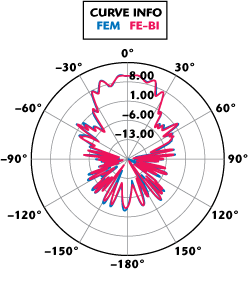
Figure 6 Antenna far-field pattern at Φ = 90° comprising the whole model.
For reference, both the FE-BI and traditional FEM results are shown in Figures 5 and 6. As is clearly seen, the agreement between the two solution methods is excellent. The accuracy of the results can be observed in Figure 5, where the electric field on the surface of the vehicle and in the cross-section is very similar. Figure 6 shows the total far-field pattern predicted by both FEM and FE-BI of the entire model, which indicates a very good agreement as well.
The same FE-BI approach can also be used to test the immunity of embedded control unit (ECU) modules. In order to demonstrate this capability, a printed circuit board (PCB) that is connected to the engine wiring harness is introduced into the simulation. The transmitted signal travels from a sensor, located at the bottom of the engine, to the PCB via a wiring harness. The wiring harness is routed from the PCB and around the engine as shown in Figure 7a. The sensor is located to the left of the graphic and the PCB is located to the right of the graphic.

Figure 7 Cable harness showing electric fields in wiring harness (a) and wiring harness attachment to PCB (b).
The wiring harness end is attached to the red four-way connector shown in Figure 7b. One of the four-way connector pins is soldered to a trace that begins in the top side of the PCB on the connector side and then goes through a via to the bottom side where it is connected to the microcontroller. For simplicity and clarity, only a single on-board diagnostic (OBD) protocol CAN#1913 signal was analyzed.
Because conductors with any given length can act as a radiation source, the wiring harness plays a vital role in EMI. To better understand the effect of the wiring harness, two simulations were performed. The first simulation contains all the above mentioned geometry as well as the car and source antenna. Figure 8 shows the results of the first simulation of the electric field based on a configuration of three wiring harness cables. For the second simulation the wiring harness is removed and, the random CAN J1939 signal is applied directly into the connector on the PCB instead of at the sensor location at the bottom of the engine. The electromagnetic fields as well as the scattering parameter of the two simulations (with and without wiring harness) are easily calculated using the FE-BI solver and are plotted in Figure 8.

Figure 8 S-matrix with the PCB alone and PCB connected to wire harness.
It is possible to observe a resonance on the PCB when it is connected to the wiring harness. The frequency of this resonance is a function of the cable length that is attached to the PCB. Additionally it is seen that the coupling between source antenna and PCB is increased when the cable harness is attached to the PCB. In this case, the wire harness increases the coupling between source antenna and PCB by over 30 dB between 152 and 191 MHz.

Figure 9 Compilation of results of both methods.
For further analysis, the electromagnetic model was dynamically linked to a circuit solver in order to simulate the CAN J1939 signal in the wiring harness and PCB. This allows engineers to seamlessly combine the frequency domain field results with time-based signals using the circuit simulator. This combination of field solver and circuit simulator makes it possible to specify all the various signals that excite the antenna and the wiring harness. For these simulations, the antenna excitation was set to a constant 150 V sinusoidal signal, with a delay of 8 μs, and a frequency sweep varying from 10 to 500 MHz. The initial time delay was set in order to clearly see the effect of the EMI on the transmitted signal. The CAN J1939 signal is generated at the sensor end of the harness for the first simulation, and injected directly at the connector (no wire harness present) for the second simulation. Figure 9 is a compilation of results for both simulations. The electric field plot distribution on the surface of the PCB substrate and at the cable is observed in Figure 9a.
The transient signal received by the microcontroller is detailed in Figure 9b. In this figure it is possible to observe the EMI from the source antenna that occurs after 8 μs. The interference is most pronounced when the PCB is connected to the harness. This is in clear agreement with the previous S-Matrix frequency response results. Figure 9c shows the eye diagram of the received signal at the microprocessor. Lastly, the bathtub diagram for the signal being received at the microcontroller for both simulations is shown in Figure 9d. As is clearly seen, the bathtub curve is greatly affected by the EMI source having a final bit error rate of 1E-2. This implies that one bit out of every 200 will be incorrectly interpreted by the microcontroller. This simulation indicates that the overall sensor system performance is going to be greatly affected by any incoming radiation at a near band that goes from 152 to 191 MHz.
With the introduction of electromagnetic numerical techniques such as HFSS FE-BI with an order of magnitude improvement in simulation speed and reduction in computational effort, simulation of a full vehicle according to automotive EMC standards is feasible. It is therefore, now possible for EMI/EMC engineers to begin to simulate entire vehicles and their subsystems in virtual anechoic chambers according to accepted EMC and EMI standards. Using simulations will also allow for accurate “what if” analysis and help engineers to determine potential EMI issues caused by driver or passenger introduced EMI/EMC sources (cell phones, Bluetooth devices, etc.). It will also allow engineers to begin to understand transient noise issues caused by the myriad of motors that are part of every vehicle.