
The availability of general-purpose harmonic-balance and Volterra-Series simulators has generated a need for accurate nonlinear models of III-V field effect transistors (FET).1 Due to the heterostructure complexity of HEMTs and the associated physical characteristics, they are most appropriately modeled based on a semi-empirical approach with parameters extracted from measurements.2
The major nonlinearities of HEMTs come from the bias-dependent drain current I-V and gate-charge Q-V relationships.3 In the past years, many equation-based large-signal HEMT models have been proposed to model those nonlinearities.1-9 Among them, the widely-used Angelov I-V model2 is one of the most successful drain current models, in virtue of its simplicity, higher-order differentiability, good convergence performances and well-defined fitting parameters. But the Angelov I-V model often faces accuracy issues, where compromises have to be made for the overall fitting.4-6 On the other hand, the charge conservative EEHEMT Q-V model7 is one representative gate charge model. Unlike the Angelov capacitance model, which may induce non-convergence during HB simulations,10 the EEHEMT charge model starts with a single gate charge formulation satisfying the principle of charge conservation to overcome the convergence problem. However, the EEHEMT model fails to model the capacitance peaking characteristics near cutoff found in GaN8 and GaAs HEMTs.9
For this purpose, an improved large-signal HEMT model is presented with the Angelov I-V model and EEHEMT Q-V model as prototypes. By maintaining the merits of the original models, the proposed model is capable of representing the nonlinear I-V and Q-V relationships between and across the entire bias range of different regimes. This has been done by introducing new modeling equations to independently control the Gm tail-off and Cgs peaking characteristics. Excellent agreement is observed between measured and simulated results by utilizing the 0.25 µm GaAs and GaN HEMT processes.
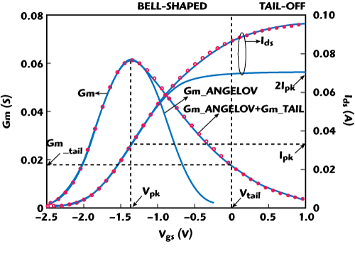
Figure 1 Graphical interpretation of the proposed non-linear I-V Model.
Model Description
Drain-current I-V Model
The Angelov I-V model2 has frequently been used to model HEMTs with typical bell-shape Gm characteristics (see Figure 1). An analytical drain-source current I-V model as an extension of the Angelov model for GaAs and GaN HEMTs is developed here. This modified I-V model is given as follows:
As described in the figure, the proposed I-V model consists of two parts: the I_Angelov part maintains the characteristics of the Angelov model, where the extraction of the key model parameters, such as the peak Gm coefficient (P1), gate voltage (Vpk) and drain current (Ipk) for maximum Gm, is still the same as in the original model. Besides, the tuning parameters in the ph function (P2 and P3) now have more freedom to model the Gm expansion when Vgs
The restriction of the “symmetrical” behavior of 2Ipk = Isat in the original Angelov model3 confines its range of operation.6 The inclusion of the I_tail current source permits the drain current to increase beyond 2Ipk as a function of Vgs and results in significantly improved accuracy. As a consequence, no trade-offs need to be made for the overall fitting,4 and the improved I-V model enhances the bias range of operation for which accuracy is maintained, as compared in the figure.
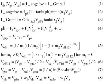
Figure 2 Complete "four-terminal" large-signal equivalent circuit of HEMTs.
In order to characterize the charge-trapping and self-heating effects3 found in most GaAs/GaN HEMTs, a four-terminal, large-signal, equivalent-circuit topology with frequency dispersion and thermal sub-circuits has been employed,11 as shown in Figure 2. The trapping and temperature coefficients as the correction of the model parameters in Equations 1 to 8 are then determined by comparing the pulsed I-V characteristics at different quiescent biasing points and ambient temperatures.12,13
Gate Charge Q-V Model
After de-embedding the extrinsic elements according to the well-known cold FET method,14 the multi-bias S-parameter measurements were used to extract the intrinsic bias-dependent gate capacitances Cgs and Cgd, and then the nonlinear gate capacitances were implemented using the charge-equation-based model as shown below:
The unified gate charge modeling equation in Equation 9 satisfies the charge-conservation principle10 to overcome convergence problem during simulations. Differentiating the gate charge expression with respect to Vgs yields the following expression for the gate capacitance C11:
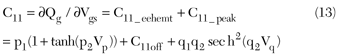
Figure 3 Interpretation of the gate charge Q-V model.
Figure 3 describes the operation of the fitting parameters. It can be seen that the additional C11_peak term, compared to the EEHEMT charge model, enables the peaking of the gate capacitance C11 near cutoff. Besides, the total gate charge Qg needs to be subdivided between the respective charge sources Qgs and Qgd, so as to be implemented into the proposed large-signal equivalent-circuit model as in Figure 2. Similar bilateral smoothing functions used in the EEHEMT charge model7 are applied here, as given below:

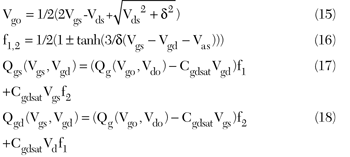
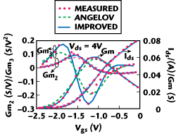
Figure 4 Measured (circles) and modeled (lines) pulsed I-V and its first three derivatives (Gm, Gm2 and Gm3) characteristics of a GaAs HEMT.
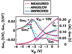
Figure 5 Measured (circles) and modeled (lines) pulsed I-V and its first two derivatives (Gm, Gm2 and Gm3) characteristics of a GaN HEMT.
Finally, the gate-source and gate-drain diodes in forward conduction are modeled using the standard Schottky diode equation.5 The complete large-signal nonlinear model is implemented in Agilent’s ADS through Verilog-A coding.
Experimental Model Verification
In order to demonstrate the usefulness of the proposed large-signal model, the 0.25 µm gate-lengths on-wafer GaAs double-heterojunction δ-doped PHEMT9 and the GaN metal-insulator-semiconductor HEMT (MISHEMT) with atomic-layer-deposited (ALD) Al2O3 gate insulator15 have been modeled and validated. As a first step, isothermal pulsed I-V measurements16 for the 2 × 100 µm gate-widths GaAs and GaN HEMTs have been investigated. The extracted drain current and its first three derivatives (Gm, Gm2 and Gm3) characteristics with respect to gate voltage are compared to measured values at the quiescent biasing point of (Vgsq, Vdsq) = (0 V, 0 V) in Figures 4 and 5, where an excellent fit is obtained for the entire bias range. These curves serve to illustrate the improvements of the derivative reproduction of the modified I-V model over the original Angelov model.
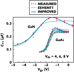
Figure 6 Measured (circles) and modeled (lines) C-V results of the GaAs and GaN HEMTs.
Furthermore, the measured gate capacitance C11 = Cgs + Cgd was evaluated from the intrinsic Y-parameters.14 The verification of the gate charge model performance (C-V) is shown in Figure 6. It can be seen that the two HEMT devices exhibit gate capacitance peaking characteristics, while the C11 of the GaN HEMT is nearly Vds independent.
The utility of the power performance of the model is verified by comparing its output predictions with measured power data. The transmitted output power characteristics at the first two harmonics and the power-added-efficiency (PAE) at a particular biasing point in deep Class AB biasing conditions are simulated and compared with measured data, as shown in Figures 7 and 8, respectively. For the GaAs HEMT, the frequency was 7.5 GHz and the bias -1.8 and 6.0 V, while for the GaN HEMT, the frequency was 4 GHz and the bias -3.7 V and 20.0 V. The input and output terminating impedances of the device were adjusted for maximum PAE performances. It can be seen that the model provides a very good prediction of the power characteristics. Moreover, the third-order intermodulation distortion (IMD3) has been characterized using two-tone tests (10 MHz spacing) under 50 Ω biasing conditions. According to the data and simulated output shown, the developed nonlinear model is capable of predicting the third-order IMD products more accurately.17
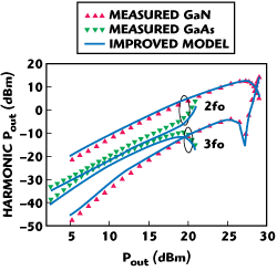
Figure 7 Measured (symbols) and modeled (lines) results for the output harmonics power levels.
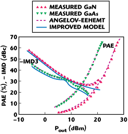
Figure 8 Measured (symbols) and modeled (lines) single tone PAE and two-tone, third order IMD performance.
Conclusion
An improved large-signal model has been presented and validated for HEMTs. Based on the well-known Angelov drain-current I-V and EEHEMT gate-charge Q-V model, two extra drain-current and gate-charge modeling sources have been proposed to independently control the Gm tail-off and Cgs peaking characteristics, respectively. The modified nonlinear model has demonstrated the ability to model the I-V and C-V characteristics of the GaAs and GaN HEMTs. In addition, the large-signal model has been implemented in Agilent’s ADS and can accurately predict the large-signal output power performances for the first two harmonics as well as third-order IMD characteristics. This model, developed from the widely-used Angelov and EEHEMT models, is easy to be extracted, and thus can serve as a useful tool in commercial nonlinear simulators.
References
- W. Curtice, “A MESFET Model for Use in the Design of GaAs Integrated Circuit,” IEEE Transactions on Microwave Theory and Techniques, Vol. 28, No. 5, May 1980, pp. 448-455.
- I. Angelov, L. Bengtsson and M. Garica, “Extensions of the Chalmers Nonlinear HEMT and MESFET Model,” IEEE Transactions on Microwave Theory and Techniques, Vol. 44, No. 10, October 1996, pp. 1664-1674.
- L.S. Liu, J.G. Ma, and G.I. Ng, “Electrothermal Large-signal Model of III-V FETs Including Frequency Dispersion and Charge Conservation,” IEEE Transactions on Microwave Theory and Techniques, Vol. 57, No. 12, December 2009, pp. 3106-3117.
- L.S. Liu, J.G. Ma and G.I. Ng, “Electrothermal Large-signal Model of III-V FETs Accounting for Frequency Dispersion and Charge Conservation,” 2009 IEEE MTT-S International Microwave Symposium Digest, pp. 749-752.
- P. Cabral, J. Pedro and N. Carvalho, “Nonlinear Device Model of Microwave Power GaN HEMTs for High Power Amplifier Design,” IEEE Transactions on Microwave Theory and Techniques, Vol. 52, No. 11, November 2004, pp. 2585-2592.
- K.S. Yuk, G.R. Branner and D.J. McQuate, “A Wideband Multiharmonic Empirical Large-signal Model for High-power GaN HEMTs with Self-heating and Charge-trapping Effects,” IEEE Transactions on Microwave Theory and Techniques, Vol. 57, No. 12, December 2009, pp. 3322-3332.
- “ADS Version ADS2005A, Documentation: Nonlinear Devices,” Agilent Technologies, Santa Clara, CA, 2005,
- J. Deng, W. Wang, S. Halder, W.R. Curtice, J.C.M. Hwang, V. Adivarahan and A. Khan, “Temperature-dependent RF Large-signal Model of GaN-based MOSHFETs,” IEEE Transactions on Microwave Theory and Techniques, Vol. 56, No. 12, December 2008, pp. 2709–2716.
- L.S. Liu, J.G. Ma, G.I. Ng and Q.J. Zhang, “Nonlinear HEMT Model Direct Formulated from the Second-order Derivative of the I-V/Q-V Characteristics,” 2010 IEEE MTT-S International Microwave Symposium Digest.
- A. Snider, “Charge Conservation and the Transcapacitance Element: An Exposition,” IEEE Transactions on Education, Vol. 38, No. 4, November 1995, pp. 376-379.
- R.G. Brady, G. Rafael-Valdivia and T. Brazil, “Large-signal FET Modeling Based on Pulsed Measurements,” 2007 IEEE MTT-S International Microwave Symposium Digest, pp. 593-596.
- K.S. Yuk and G.R. Branner, “An Empirical Large-signal Model for SiC MESFETs with Self-heating Thermal Model,” IEEE Transactions on Microwave Theory and Techniques, Vol. 56, No. 11, November 2008, pp. 2671-2680.
- A. Jarndal and G. Kompa, “Large-signal Model for AlGaN/GaN HEMTs Accurately Predicts Trapping- and Self-heating-induced Dispersion and Intermodulation Distortion,” IEEE Transactions on Microwave Theory and Techniques, Vol. 54, No. 11, November 2007, pp. 2830–2836.
- G. Dambrine, A. Cappy, F. Heliodore and E. Playez, “A New Method for Determining the FET Small-signal Equivalent Circuit,” IEEE Transactions on Microwave Theory and Techniques, Vol. 36, No. 7, July 1988, pp. 1151-1159.
- Z.H. Liu, G.I. Ng, S. Arulkumaran, Y.K.T. Maung, K.L .Teo, S.C. Foo, V. Sahmuganathan, T. Xu and C.H. Lee, “High Microwave-noise Performance of AlGaN/GaN MISHEMTs on Silicon with Al2O3 Gate Insulator Grown by ALD,” IEEE Electron Device Letters, Vol. 31, No. 2, February 2010, pp. 96-98.
- “DiVA [Dynamic I-V Analyzer],” Nanometrics Inc., Milpitas, CA, 2008. Available: www.nanometrics.co.kr/products/Diva.html
- S.A. Maas, “How to Model Intermodulation Distortion,” 1991 IEEE MTT-S International Microwave Symposium Digest, pp. 149-151.
Lin-Sheng Liu received the bachelor’s degree (with honors) in electronic engineering from the University of Electronic Science and Technology of China (UESTC), Chengdu, China, in 2005, and is currently working toward his Ph.D. degree in circuits and systems at UESTC. His current research interests include the characterizations/ modeling of III–V compound semiconductor devices and high-efficiency switch-mode PA design.