
There has been a widespread trend toward higher levels of integration in microwave and millimeter-wave system design, motivated by a desire to reduce cost, size and complexity, particularly as many old applications are being re-invented in array architectures. The most commonly used format for achieving high levels of integration in millimeter-wave systems is the MMIC-based multi-function module (MFM). High performance MMIC circuits of all kinds up to about 50 GHz are already readily available at low cost from many commercial suppliers. The selection of commercial MMICs above 50 GHz is more limited, however, although new ones are introduced regularly, and foundry services for III-V semiconductors are provided by many companies that enable users to design their own custom chips for applications well over 100 GHz.1
The MMIC approach does have limitations, of course, not the least of which is relatively low-Q for passive components like filters. Microstrip filters are the most common form of integrated filter used with MMIC technology. They can be made on-chip along with an amplifier, mixer, multiplier, or other active circuit, or they can be printed separately on a ceramic substrate like alumina. The latter approach is usually most economical since real estate on III-V semiconductor wafers is costly compared to that of passive substrates, and they can easily be packaged alongside other MMICs and connected with bond wires just like any other chip. The microstrip approach is suitable for most low pass filters and band-pass filters that require wider stop bands than can easily be accomplished with waveguide. The Q of microstrip filter resonators is often not very good, however, and high order filters with more than 4 or 5 poles are usually not practical. In addition, the stop-band attenuation of microstrip filters is limited in extreme cases by the MMIC housing rather than the filter itself. For rejection larger than about 30 dB or so, extreme care must be taken in the design of the cavity in which the chip is mounted to prevent leakage over or around the chip from exceeding that limit.
For systems that have stringent requirements for low insertion loss, steep band edges, or very high out-of-band rejection, it is usually necessary to implement filters in waveguide. For most highly integrated systems, this has meant that the filter becomes a necessary breaking point between multi-function modules. Since it is not uncommon for the various input and output connectors to overwhelmingly dominate the size of a MMIC-based module, the ability to incorporate these high-Q filters entirely within the module and eliminate two waveguide flanges would represent a significant savings in both size and complexity. Two complementary approaches for integrating waveguide filters within MMIC modules have been studied and are presented in this article. First, however, the transition from printed circuit to waveguide, which is utilized in both filter structures, is reviewed.
Microstrip-to-waveguide Transition
Whether the filter is integrated into an MMIC-based module or not, it is necessary to first transition from microstrip or CPW transmission line to waveguide. The longitudinal E-field probe is a reliable and widely used transition, which can be matched over the full waveguide bandwidth. This transition uses a planar probe that extends partway into the guide along the E-plane in the middle of the broad wall, centered about a quarter-wavelength from the guide back short, as shown in Figure 1. A simple microstrip-matching network outside the guide, consisting of a short inductive transmission line and a low impedance quarter-wave transformer, provides a good match (better than 20 dB return loss) over the full rectangular waveguide bandwidth.2,3 The required transmission line dimensions are not extreme, and this probe can be inexpensively fabricated in large quantities using common alumina or other printed-circuit fabrication technologies. Because the probe is located at or near the center of the broad wall, the housing can be split at the waveguide’s symmetry plane for minimum loss.
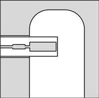
Fig. 1 E-plane longitudinal probe.
The insertion loss of this transition is typically a few tenths of a dB. The need for two such transitions, one at either end of the filter, detracts slightly from the almost lossless performance of waveguide components, but is still not a dominant source of loss in high order filters. In addition, since the transition loss is essentially flat with frequency, the steepness of the band edges and very high stop-band rejection achievable with waveguide filters remain intact.
The overall utility and easy implementation of these probe transitions have made them a common component in many millimeter-wave module designs, and are very often the first and last elements in the RF chain within a module. They now form a crucial part of the integrated waveguide filters that are discussed in the following sections.
E-plane Shim Filters
The first topology that was used for completely internal, MMIC-to-MMIC waveguide filters was the E-plane septum, or “Shim” filter.4 As illustrated in Figure 2, this structure is comprised of a series of thin metal vanes that run vertically from the center of one broad wall of the guide to the other. Each vane, or septum, acts as a shunt inductive discontinuity whose magnitude is determined by the length of the vane in the direction of propagation.

Fig. 2 Conceptual structure of the E-plane septum filter.
For analytical purposes, these reactive elements may be treated as impedance inverters, spaced at approximately half-wavelength intervals on the main transmission line. The desired inverter parameters, Ki, may be determined easily from readily available Tchebyscheff or other appropriate filter prototypes.5 These inverter parameters may then be translated into physical dimensions of the septa, using empirical formulas or electromagnetic simulation. As the design of E-plane filters is already well understood and described in the literature,4–7 it will not be repeated here. The focus instead will be on their integration into multi-function modules.
Fig. 3 Illustration of a multi-function module using E-plane shim filters.
Figure 3 is an illustration of an existing MMIC multi-function module that uses internal shim filters, and serves as a good example of how they are constructed. Straight waveguide “grooves” are machined into both halves of the split block for each filter (in this case four). These grooves do not extend to the outer edge of the block, where there would normally be a flange for connection to other components in the system, but instead run from one back short to another, with the aforementioned probe transitions at either end. Held between the two halves of the split block is a “shim card,” a piece of metal shim stock that has been chemically etched by a lithographic process. This manufacturing process is available commercially, and can easily achieve dimensional tolerances less than 25 ?m. Alignment of the shim card and the top- and bottom-halves of the split block with one another is ensured by the use of dowel pins.
The module shown is a dual-channel Ka-band down converter for the Deep Space Network (DSN) array. Narrow filters were needed for the communication bands at 32 and 37.5 GHz. The requirements on these filters precluded the use of microstrip, but were a good match to the potential performance of integrated E-plane shim filters.
The 32 GHz filter was thus designed for WR-28 waveguide, while the 37.5 GHz filter was made for WR-22. WR-22 was selected for the higher frequency filter, even though WR-28 would have worked for both, because the upper stop band is limited to those frequencies for which the guide is single-moded, so it makes sense to choose guide dimensions that put the desired pass band as close to the bottom of the waveguide band as possible. Since the waveguides are completely contained within the module, it would have been reasonable to design the filters around custom waveguide dimensions. It was decided, however, to stick with standard guide dimensions this time so that existing (proven) longitudinal probes could be used and the filters could be easily tested (in another chassis) in case something went wrong in the first attempt.
Before a filter card was made for the final module, several test filters were made without the probes or the rest of the MMIC chips in order to provide a basis for comparison, as well as to explore the accuracy of filter simulations and manufacturing tolerances. The shims made were 50 mm thick and were gold-plated to minimize loss in the contact with the chassis. One of the test pieces is shown in Figure 4. Measurements for two of the test filters are shown in Figure 5. The insertion loss in the pass band was approximately 0.5 dB at 32 GHz and 0.8 dB at 37.5 GHz. The initial filters were tuned somewhat low due to over-etching of the shim card, but once this was taken into account, the measurement and simulation were in excellent agreement.

Fig. 4 Open test block and shim card.

Fig. 5 Measured insertion loss for the 32 and 37.5 GHz shim filters.
A series of simulations were run with Ansoft HFSS™ to explore the effects of manufacturing and assembly errors on the frequency response. The largest potential source of error turned out to be imprecise etching of the shim. Both measurement and simulation indicated that filters in this frequency range (30 to 40 GHz) would detune at a rate of approximately 6 MHz per micron of over- or under-etching. The precise number, of course, depends on the waveguide dimensions chosen.
The second largest source of error turned out to be the waveguide width, or from the machinist’s perspective, the depth of the grooves in the split block. Groove depth errors in these bands should detune the filters at a rate of approximately 4 MHz/?m.
Finally, misalignment of the shim with the features on the split block can detune the filter at a rate of approximately 0.3 MHz/?m. This mechanism is essentially controlled by the diameter of the through-holes in the shim card for the dowel pins. If the holes are too large, the shim will not be as precisely aligned with the waveguide; if they are too small, however, it will be difficult to get the shim to fit over the pins without bending it. In practice, an increase of 50 mm over the pin diameter was found to be large enough for an easy slip-fit over the pins, while tight enough that misalignment was not a significant source of error in the filter’s frequency response.
Other possible detuning mechanisms, such as waveguide height errors and shim thickness, were explored, but were found to be negligible compared to the factors described above. None of the factors explored had a significant effect on filter bandwidth.
After taking all these detuning mechanisms into account, along with the expected manufacturing tolerances, it was found that the center frequency of the filters might be off by as much as 150 MHz in either direction. Therefore, the final filters were designed to have a 300 MHz excess bandwidth to allow for this shifting.
Field tuning of the filter is possible by using dielectric rods that extend into the waveguide from the narrow wall into the space between septa. To effectively shift the center frequency without distorting the band shape, these rods must be inserted into all the cavities (spaces between the septa) of the filter. Dielectric tuners (rods) with threaded heads are available commercially for this purpose, although care must be taken to choose tuners that are narrow enough such that their access holes are cutoff in the frequency band of the waveguide. The tuning range may then be extended by having more than one tuner per cavity. This functionality may be implemented if necessary after the module has already been machined by threading the necessary access holes from the outside of the block.
Among the secondary advantages of this approach is the ability to reconfigure the filter response simply by opening up the module and replacing the shim card with a new design. No other components would need to be replaced or redesigned. The only constraints on the interchangeability of filter designs are that they use the same waveguide cross-section and fit within the length of the grooves provided. The shim card may even be left out altogether, effectively creating a “through” (limited to the waveguide bandwidth) in place of the filter for test and debugging purposes.
A limitation of the E-plane shim filter is that it cannot be used for relatively wide pass bands. The effective reactance of a shorting metal strip in a waveguide, even a very narrow strip, is far too large for broadband filters. Attempts to design a shim for such a broadband response forces the outermost strips to be very thin, beyond the range of validity for empirical equivalent circuit formulas, and impractical to implement in any case. Another filter structure was found to be more suitable for broad bandwidth cases, and is discussed in the following section.
Thick-iris Direct Coupled Cavity Filters
A common form of waveguide filter is the inductive-iris coupled cavity resonator filter.5 Typically, this structure has been made by cutting very narrow slots at roughly half-wavelength intervals in the narrow walls of a section of waveguide, and then inserting metal shims into these slots to form thin inductive irises that separate a number of cavity resonators. The filters discussed in this section are simply an adaptation of that structure which allows it to be machined directly into the housing of a split block.
In order to keep the waveguide losses to a minimum, a split body should have all waveguides split at the midpoint of the broad wall wherever possible, as symmetry of the TE10 mode ensures that no current crosses this boundary. From the machinist’s perspective then, an inductive iris looks like a metal wall rising vertically from the groove in either half of a split block, separating open cavities that are as tall as the narrow wall of the guide and as deep as half the broad wall. Practical constraints on the machining of such a structure require that the thickness of this wall be much thicker than would normally be used for an inductive iris. In practice, a wall thickness of 500 mm for filters in the 40 to 50 GHz range has been used. Furthermore, to ease manufacturability, the depth of the cut should only be about 1.5 times the diameter of the end-mill used. For example, a WR-19 waveguide groove would be 2385 mm deep in the split-block, and would be cut with a 1590 mm diameter mill, leaving corners with a radius of 795 mm. The resulting appearance of a typical iris in a WR-19 guide is shown in Figure 6.

Fig. 6 500 um thick iris with radiused corners in a WR-19 waveguide.
A wall 500 ?m thick in the middle and widening to more than 2090 mm at the top and bottom of the guide clearly does not look much like the “thin” iris walls described by the classic empirical formulas.8 Fortunately, the structure can still function as an impedance inverter, but its equivalent circuit must be derived by EM simulation. This is done by first simulating a number of irises, with dimensions subject to the manufacturing constraints previously described, and with a wide range of wall heights varying from 0 to almost the full depth of the groove. Setting the reference planes to the center of the wall (zero-length through), the inverter parameters for each wall height may then be calculated using the expressions5

where X11 and X12 are the imaginary parts of the impedance parameters Z11 and Z12, respectively (the real parts should be 0 for a lossless, reciprocal network). These calculations need only to be done at the center frequency of the filter to be designed. As such small simulations run very quickly, it does not take long to accumulate enough data points to create best-fit curves that describe K and f as a function of wall height. These curves may then be used to select iris dimensions for the inverter K-parameters derived from filter prototypes as described in Matthaei, Young and Jones.5 The phase parameters, ?, must then be used to correct the spacing between these irises, nominally ?g/2.

Fig. 7 Layout of the EVLA Ka-band down converter using a thick-iris waveguide filter.
An example module in which this type of filter is used is shown in Figure 7. The module is approximately 5 by 5 cm. Like the module presented in the previous section, this is also a Ka-band down converter, this time for the Expanded Very Large Array (EVLA). The filter follows a broadband tripler, which is used to generate the 43.5 to 49.5 GHz local oscillator within the module. The tripler rejects even harmonics well, but a filter is needed to attenuate the first and fifth harmonics. The fundamental tone is a concern because it falls directly within the wide IF band of the receiver, and the fifth is a problem because it forms a spur within the image band of the mixer. The required rejection was too steep for a microstrip filter, and the bandwidth was too large for the E-plane septum filters described earlier. Thus, a thick-iris filter was pursued instead.
WR-19 was selected for this filter since its cutoff frequency is just below the pass band of the filter, thus ensuring maximum rejection in the lower stop band and the widest possible upper stop band (defined by the onset of over-moding in the guide). To begin, a number of thick-iris inverters with radiused corners were simulated with varying wall heights. These results were then used to find iris dimensions that match the desired K values for an ideal half-wave filter derived from a six-pole, 0.1 dB ripple, Tchebyscheff prototype. Finally, the cavities were made to have electrical length of 180° minus the effective inverter phase ? at either end.

Fig. 8 Final dimenstions for the 43.5 to 49.5 GHz integrated thick-iris filter.
The outermost irises of the filter in this example included a transition from WR-19 to WR-22. This was done in order to take advantage of the WR-22 longitudinal probes that already existed. The final dimensions (in mm) of this filter are shown in Figure 8. As before, a filter test block was made to verify the design before machining it into the final down converter chassis. The simulated and measured results for the filter are shown in Figure 9. The excellent agreement between theory and measurement at millimeter-wave frequencies demonstrates the reliability of this technique.

Fig. 9 Simulated and measured performance of the 43.5 to 49.5 CHz thick-iris filter.
In order to fairly evaluate the performance of these integrated waveguide filters in a MMIC-to-MMIC environment, one must take into account the loss of the probe transitions at either end. A comparison of the mid-band insertion loss for simple microstrip filters and integrated waveguide filters is shown in Figure 10. For this example, the Q of the microstrip resonators is assumed to be 100, which is fairly typical for the lower millimeter-wave band. The Q of the waveguide resonators is assumed to be 1500, but the two probes are estimated to add 0.5 dB each to the loss of the filter. As the figure shows, for filters with more than 3 or 4 poles, the waveguide filters described in this article have a clear advantage in terms of loss. In addition, the waveguide filters will have better peak stop-band rejection than can normally be achieved with open transmission lines like microstrip.

Fig. 10 Comparison of the theoretical mid-band insertion loss for microstrip and integrated waveguide band-pass filters.
A chief disadvantage of the waveguide structure is its limited stop-band width, caused by over-moding. Note that the second pass band begins around 65 GHz, which corresponds approximately to the first cutoff frequency of high order modes in WR-19 waveguide. Wider stop bands are theoretically possible by employing a waffle-iron structure,5 but the necessary geometry is difficult to machine within a typical MMIC housing. Should such a wide stop band be needed, a simpler solution would be to combine a low order, low pass microstrip filter in cascade with a high order, band-pass waveguide filter as described in this article.
Conclusion
This article has demonstrated techniques for integrating two types of high performance waveguide filters within the body of a MMIC-based multi-function module. While based on well-known and widely used filter structures, some details of their construction have been modified to allow for their fabrication in a package designed for MMICs.
Acknowledgments
The authors wish to acknowledge FotoFab, Precision PhotoFab and Quinstar for fabrication of the components for the shim card filters. Thanks also to Niklas Wadefalk for providing the layout of the EVLA down converter. This work was carried out in part by the Jet Propulsion Laboratory, California Institute of Technology and by the National Radio Astronomy Observatory. The National Radio Astronomy Observatory is a facility of the National Science Foundation operated under cooperative agreement by Associated Universities Inc.
References
1. M. Morgan, Millimeter-wave MMICs and Applications, PhD Thesis, California Institute of Technology, May 2003.
2. Y.C. Leong and S. Weinreb, “Full Band Waveguide to Microstrip Probe Transitions,” IEEE MTT-S International Microwave Symposium Digest, Anaheim, CA, 1999, pp. 1435–1438.
3. S. Weinreb, T. Gaier, R. Lai, M. Barsky, Y.C. Leong and L. Samoska, “High Gain 150 to 215 GHz MMIC Amplifier with Integral Waveguide Transitions,” IEEE Microwave and Guided Wave Letters, Vol. 9, July 1999, pp. 282–284.
4. Y. Konishi and K. Uenakada, “The Design of a Band Pass Filter with Inductive Strip-planar Circuit Mounted in Waveguide,” IEEE Transactions on Microwave Theory and Techniques, Vol. 22, No. 10, October 1974, pp. 869–873.
5. G. Matthaei, L. Young and E. Jones, Microwave Filters, Impedance-matching Networks and Coupling Structures, Artech House Inc., Norwood, MA, 1980.
6. G. Goussetis, A. Feresidis, D. Budimir and J. Vardaxoglou, “A 3rd Order Ridge Waveguide Filter with Parallel Coupled Resonators,” IEEE MTT-S International Microwave Symposium Digest, Fort Worth, TX, 2004, pp. 595–597.
7. V. Postoyalko and D. Budimir, “Design of Waveguide E-plane Filters with All-metal Inserts by Equal Ripple Optimization,” IEEE Transactions on Microwave Theory and Techniques, Vol. 42, No. 2, February 1994, pp. 217–222.
8. N. Marcuvitz, Waveguide Handbook, Peter Peregrinus Ltd., London, UK, 1993.
Matthew A. Morgan received his BSEE degree from the University of Virginia, Charlottesville, VA, in 1999, and his MS and PhD degrees in electrical engineering from the California Institute of Technology, Pasadena, CA, in 2001 and 2003, respectively. He is currently a research engineer with the National Radio Astronomy Observatory (NRAO), Charlottesville, VA, where he is involved in the design of monolithic millimeter-wave integrated circuits (MMIC) and multi-chip modules (MCM) for radio telescope arrays.
Sander Weinreb received his BSEE and PhD degrees from the Massachusetts Institute of Technology (MIT), Cambridge, MA, in 1958 and 1963, respectively. He is currently a principal scientist with the Jet Propulsion Laboratory (JPL), Pasadena, CA, and a faculty associate with the California Institute of Technology, Pasadena, CA. Prior to this, he was a research professor with the department of physics and astronomy at the University of Massachusetts. His main area of research is the development of low noise microwave and millimeter-wave integrated circuits (MMIC) for use in radio astronomy and atmospheric research.