
In full-duplex communication systems such as W-CDMA, a receiver’s tolerance to unwanted transmit signals, including a co-located transmitter, is significantly important since transmission and reception occur simultaneously. Since transmit signals can be as little as 30 MHz away in frequency from the receive signal, surface acoustic wave (SAW) filters are typically employed to reject such close-in interferers. The receiver’s low noise amplifier (LNA) must accommodate all signal levels delivered at the SAW filter output. In this article, a highly signal-tolerant LNA is designed, with a worst-case 1 dB compression point (P1dB) of -11 dBm, a gain (S21) of over 17 dB and a noise figure (NF) close to 2.6 dB, for implementation in 0.35 mm, 4-metal CMOS technology.
A conventional direct conversion receiver is described in Figure 1, in which a common antenna is used for both transmission and reception of the radio signal. The commonpath to the antenna is established by the duplex filter and further filtering is provided by individual transmit and receive filters as required. In a full-duplex W-CDMA system, the maximum power amplifier (PA) output power is 29 dBm, which will find its way to the receiver via the duplexer, as shown in the Figure.

Figure 1 System diagram of a direct conversion receiver.
From W-CDMA 3GPP specifications,1,2 the maximum signal at the input to the receiver is -25 dBm at the low gain setting and -43 dBm at the high gain setting. An LNA filter therefore has to attenuate the transmitter signal by at least 43 + 29 = 72 dB, when operating the LNA at the prescribed -43 dBm, in order to prevent the LNA from being compressed by the transmitter signal.

A filter that produces 72 dB of attenuation of the transmission signal will inevitably require a considerable amount of poles, which in turn would imply that the wanted frequency band itself will be subjected to losses due to this filtering process. By improving the linearity of the receiver path and in particular the LNA, it is possible to implement a low-loss filter with fewer poles. Fewer poles in the receive path inevitably means a filter with reduced signal loss at the wanted receiver frequency, thereby resulting in an increase in sensitivity of the receiver. By considering a highly linear LNA, with an input P1dB of -14 dBm or better, the SAW filter in the receive path can be removed, thereby substantially reducing receiver path losses and reducing component count and cost of the receiver (see Table 1).

Figure 2 LNA circuit diagram.
The Method of Achieving the Increased Compression Point
In the power amplifier world, highly linear amplifiers are designed such that the transistor is biased either at the class B or class AB bias points. In this work, the same technique is employed to achieve a highly linear LNA, by biasing the transistor at the class AB bias point. This technique, however, lowers the transconductance (gm) value, reducing the gain of the transistor and improving its dynamic range. The design is structured in two stages: A first-stage cascode amplifier, biased to a point just above the threshold voltage, followed by a second-stage PMOS amplifier. As illustrated in Figure 2, the LNA consists of an input cascode section and a second-stage drain follower. The cascode section consists of two NMOS devices M1 and M2 and an LC parallel resonant circuit consisting of L2 and C1.
The transistor M1 is a common-source amplifier that is biased just above its threshold voltage. The function of M1 is essentially to convert the input signal voltage into an equivalent drain current ID1. The transistor M2 is a common-gate amplifier that provides isolation between the input to the amplifier and the output to capacitor C2 and thus reduces the Miller capacitive effect.4 The inductor L2 and capacitor C1 are chosen such that they have a parallel resonance at the chosen frequency of operation, thus providing maximum voltage gain at the receiver frequency, while rejecting frequencies outside this band, including the amplified co-located transmitter signal.
The amplifier second-stage consists of a PMOS device M3 and an LC resonant circuit. Here again L3 and C3 are chosen such that they resonate at the frequency of operation and reject frequencies outside of this band, including the amplified co-located transmitter signal. In addition, the second stage of the LNA provides:
- Isolation between the first-stage load and the down-conversion mixer input impedance, thereby maximizing the first-stage cascode amplifier’s load impedance.
- The PMOS device hole mobility is typically one-quarter of the electron mobility of the NMOS device, improving tolerance to larger signals.
A PMOS device has an increased thermal noise contribution when compared to an equivalent NMOS device. The noise effect of the PMOS device is reduced, however, by the gain of the previous NMOS cascode stage, with a net total LNA noise figure defined by the Friis formulae.5
Design of the LNA
Due to the duplexer filter impedance-matching requirements at the input of the LNA, the input impedance is set to 50 Ω. Given that the output of the LNA is to be connected to a down-conversion mixer of approximately 200 Ω input impedance, the output of the LNA is matched to this value. The biasing and gain calculations of the input first-stage cascode amplifier are based on the linearity requirements due to the presence of the unwanted transmitter signal. Table 2 is derived from the values obtained from the process manual.6

A calculated gain of approximately 9.3 dB is obtained with a drain current of just less than 1 mA, in the absence of an input signal. With the RF signal present, the bias and gain vary; the current variation with applied signal is presented later in the article.
The second-stage PMOS drain follower amplifier is also biased in the class AB mode, but the final bias is set according to the amount of transmitter signal attenuated by the parallel resonance circuit L2 and C1 of the input cascode amplifier. The design is then implemented in the simulator in schematic form, as indicated in Figure 3.

Figure 3 Schematic diagram of the simulated LNA.
The circled sections indicate the parallel resonance circuits. The input inductor, L1, is implemented as a bondwire inductor and therefore external to the schematic entry. The initial bond-wire inductance, LBW, was chosen as 5 nH, based on the rule of thumb of 1 nH per mm, and then calculated using the Greenhouse formulae.7 An on-chip inductor is not implemented in this design as they are generally of lower Q and hence high NF contribution, due to the increased ESR value.

Figure 4 Simulated input and output return losses.

Figure 5 Measured input and output return losses.
Simulated Input and Output Return Loss
Figure 4 shows the log magnitude plot of the input and output return losses. The input return loss (S11) is better than -17.5 dB and the output return loss (S22) is better than -13 dB over the receive frequency range of 2.11 to 2.17 GHz. Both simulations include the effects of substrate coupling and other parasitic effect from the extracted layout.
Measured Input and Output Return Losses
Figure 5 shows the measured input and output return losses of the LNA, measured with a network analyzer. The S11 is better than -12 dB and the S22 is better than -9.8 dB over the receive frequency range of 2.11 to 2.17 GHz. The measured results marginally differ from the simulated results as they display a slight shift in center frequency resonance.
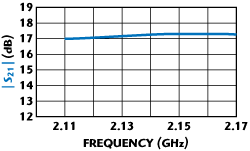
Figure 6 Simulated voltage gain of the LNA.
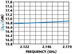
Figure 7 Measured voltage gain of the LNA.
Simulated and Measured LNA Gain
The forward gain plot shown in Figure 6 indicates a consistently flat gain between 17 and 17.25 dB over the frequency band of interest, with the gain peaking at approximately 2.15 GHz, which is the center of the receive frequency band.
The plot shown in Figure 7 indicates a forward gain between 16.75 and 16.9 dB over the frequency of interest. The gain is slightly higher at 2.17 GHz and slightly lower at 2.11 GHz and is primarily due to the better input return loss at that frequency.
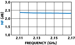
Figure 8 Simulated noise figure of the LNA.

Figure 9 Measured noise figure of the LNA.
Simulated and Measured LNA Noise Figure
The simulated LNA noise figure in Figure 8 shows that the NF is just under 2.4 dB across the frequency band of interest and is uniformly flat. This is desirable as it is a further indication of a uniform sensitivity of the receiver over the entire receive frequency band.
The measured LNA noise figure shown in Figure 9 shows that the NF is less than 2.45 dB for the frequency band of interest and falls by less than 0.1 dB at the higher frequency of 2.17 GHz.

Figure 10 Simulated P1dB compression point of the LNA.

Figure 11 Measured P1dB compression point of the LNA.
Simulated and Measured LNA P1dB
Figure 10 shows the simulated input referred 1 dB compression point of the LNA. The simulation was performed at the center frequency of 2.14 GHz, which is the mid-channel frequency for the receiver channel.
Figure 11 shows the input referred 1 dB compression point of the LNA. The measurement was performed at the center frequency 2.14 GHz, and was found to be -11.6 dBm. It is comfortably larger than the calculated requirement of -14.4 dBm (see Table 1), but slightly worse than the simulated value of -10.8 dBm. The compression point curve also shows a slight gain expansion prior to compression and is a characteristic commonly seen in class AB power amplifiers.
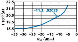
Figure 12 LNA current consumption vs. input power.
LNA Current Consumption Analysis
Figure 12 shows the current consumption of the LNA. Since the bias is an AB type, the signal input level has an effect on the bias point. The current is dependent on the input signal level for levels higher than -25 dBm. For width selection and sizing purposes due to problems with electromigration, the maximum current consumption at 2.7 V supply is 20.25 mA.
Conclusion
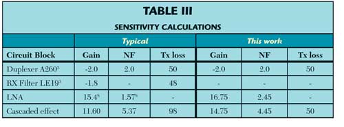
A suitable method has been developed to design a highly linear receiver LNA that can down-convert high power signals in conformance to modern wireless standards. The increased linearity of the LNA and the subsequent filtering provided by the tuned load impedances allows an increasing sequential rejection of interference signals through the LNA sections. The slight increase in NF, due to the biasing technique implemented, allows for a lower system NF for the entire receiver due to the reduced receiver filtering requirements. As demonstrated in Table 3, a cascaded NF of 4.45 dB and a gain of 14.75 dB is achievable.
References
- The 3 GPP UMTS Standard; available online at http://www.3gpp.org.
- O.K. Jensen, T.E. Kolding, C.R. Iversen, S. Laursen, R.V. Reynisson, J.H. Mikkelsen, E. Pedersen, M.B. Jenner and T. Larsen, “RF Receiver Requirements for 3G W-CDMA Mobile Equipment,” Microwave Journal, Vol. 43, No. 2, February 2000, pp. 22-46.
- EPCOS Components; available online at http://www.usa.epcos.com/Web/share/all/files/RFProducts/WCDMA.pdf.
- T.H. Lee, The Design of CMOS Radio-Frequency Integrated Circuits, Second Edition, Cambridge University Press, New York, NY, 2004, p. 248.
- H.T. Friis, “Noise Figure of Radio Receivers,” Proceedings of the IRE, Vol. 32, No. 7, July 1944, pp. 419-422.
- Austriamicrosystems™ Process Manual, ENG-182 rev. 4, pp 12-24; available online at www.austriamicrosystems.com.
- H.M. Greenhouse, “Design of Planar Rectangular Microelectronic Inductors,” IEEE Transactions on Parts, Hybrids, and Packaging, Vol. 10, No. 2, June 1974, pp. 101-109.