
Phased-array radars, wireless communication transmitters, including public safety radio networks, medical instrumentation and other various traditional civil and military applications, require demanding performance of microwave power transistors. The broadband operating capability is always demanding in various RF circuits and subsystems. Wireless systems deliver high data rate signals to provide multimedia and broadband connectivity. This demanding performance of power amplifiers in a system should cover wide bandwidth and at the same time have a high linearity to amplify the signals without distortion. In combination with these properties, the high efficiency is also important, especially with the mobile systems, where cooling is additional and of relatively higher cost on the system. The next generation cell phones also require wider bandwidth and improved efficiency. These high power and high frequency applications require transistors with a large breakdown voltage, high electron velocity and high thermal conductivity. Therefore, a wide bandgap (WBG) semiconductor such as GaN is a favorable choice.1
The high output power density of GaN transistors allows the fabrication of much smaller devices compared to Si and GaAs. A higher impedance, due to the smaller size, allows for easier and lower loss matching networks in amplifiers. The wider bandgap also enables the electronics to operate at elevated temperatures. These features in amplifiers, enabled by the superior semiconductor properties, make GaN a promising candidate in microwave power applications.
Due to these superior electronic properties of GaN semiconductor and the possibility to utilize SiC substrate, which has a high thermal conductivity (3.5 to 4.9 W/cm K), a power density as high as 30 W/mm at 4 GHz2 as well as an output power of 500 W at 1.5 GHz3 have already been demonstrated. An output power of 75 W for a packaged single-ended GaN-FET has been reported under pulsed conditions for L/S band applications.4 The introduction of GaN HEMTs on silicon substrates is considered to be a great development for reducing the cost of these transistors. Therefore, these transistors are also expected to replace some Si LDMOS designs in the telecommunications sector. GaN technology has already been used in power amplifiers for mobile base station applications, and a number of manufacturers and researchers have reported high efficiencies, output powers and power densities.5-10
In this article, the results of two fabricated power amplifiers in two different GaN HEMT technologies are presented. The purpose of this work is to explore the broadband performance and capabilities of these transistors for PAR and EW systems.
Power Amplifier Designs
Power Amplifier Using GaN HEMT on Silicon (PA1)

Figure 1 Schematic of the fabricated PA1 amplifier.
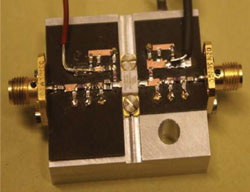
Figure 2 Photograph of the PA1 amplifier.
A hybrid amplifier operating in the 0.2 to 1.8 GHz band for phased-array transmitters has been designed and fabricated. The design is based on a large-signal model of packaged 25 W (wideband 15 W) GaN HEMT on Si from Nitronex. The actual designed bandwidth is wider than the amplifier described in the next section. It has lumped matching networks (without feedback) built on Rogers Duroid 5880 substrates. The amplifier is first designed using ideal components, which were later replaced by their models and S-parameter blocks. An unconditional stability is obtained by adding a parallel combination of resistor R1 and capacitor C5 in series to the input matching network. The schematic diagram and picture of the fabricated amplifier are shown in Figures 1 and 2, respectively.
Hybrid Power Amplifier Using GaN HEMT on SiC (PA2)

Figure 3 Schematic of the fabricated PA2 amplifier.
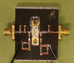
Figure 4 Photograph of the PA2 amplifier.
A 0.7 to 1.8 GHz hybrid amplifier for high power phased-array transmitter applications have been designed and fabricated. This amplifier is based on a packaged 10 W GaN HEMT from Eudyna. It has lumped matching networks (with feedback) built on the same Rogers Duroid 5880 substrate. A parallel combination of resistor R1 and capacitor C3 in series to the input matching network is added in combination with feedback to enhance stability, increase the bandwidth and reduce distortion. The feedback network consists of a capacitor Cfb and total resistor of 80 V. The resistor is divided between two 1206 SMT resistors Rfb1 and Rfb2 to enhance power tolerance. It was very difficult to obtain unconditional stability without feedback for this amplifier. A schematic diagram and picture of the fabricated amplifier are shown in Figures 3 and 4, respectively.
Results and Discussion
Simulation and Measured Results for the Fabricated PA1

Figure 5 Simulated and measured small-signal performance of PA1.
The simulated and measured small-signal gain S21 and input reflection coefficient S11 showed good agreement over the entire frequency band. A gain greater than 15 dB is achieved for the entire frequency band. The design shows matching below -4 dB for S11 and below -7 dB for S22, as shown in Figure 5. The output reflection coefficient S22 shows good agreement up to 500 MHz and, at higher frequencies, measured results are better than the simulation. There is also frequency shift at the upper band, which could be because of some minor error in the output matching network for higher frequencies or due to some minor error in the large-signal model. The design shows unconditional stability at all simulated frequencies. The class AB bias point used was Vg = -1.5 V and Vd = 28 V with a quiescent drain current of 230 mA.
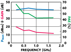
Figure 6 Power measurements at Vd = 28 V for the PA1 amplifier.
Power measurements were performed at five different frequencies from 0.2 to 1.8 GHz and the results are shown in Figure 6. A maximum output power of > 40.6 dBm (11.5 W) with a power gain of ≤ 11 dB is obtained at all measured frequencies. A maximum output power is obtained at 700 MHz, which is 42.52 dBm (~18 W) and a maximum PAE of 66 percent with a maximum gain of 19.5 dB is obtained at 200 MHz. The measured output power is almost constant at all measured frequencies as shown in the figure.

Figure 7 Two-tone test results for PA1 at 1 GHz with a tone spacing of 4 MHz.
A two-tone inter-modulation distortion measurement was carried out at 1 GHz. The separation between the two carrier tones was 4 MHz. The IMD3 at 10 dB back off the P1dB was -31 dBc and the output IP3 was 48 dBm. The results are shown in Figure 7.
Simulation and Measured Results for the Fabricated PA2

Figure 8 Simulated and measured small-signal performance of PA2.
Simulated and measured S-parameters showed good agreement up to approximately 1.4 GHz. Above this frequency the measured small-signal gain starts to decrease compared to the simulation. The gain achieved is greater than 10 dB up to 1.4 GHz and is above 9 dB across the remainder of the band. The design showed an input matching below -4 dB (for S11) and below -10 dB at the output (for S22), as shown in Figure 8. The design shows unconditional stability at all simulated frequencies. The class AB bias point used was Vg = -0.4 V and Vd = 48 V with a quiescent drain current of 270 mA.
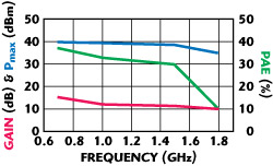
Figure 9 Power measurement results of PA2 at Vd = 48 V.
Power measurements were performed at four different frequencies from 0.7 to 1.8 GHz and the results are shown in Figure 9. The maximum output power, measured at 700 MHz at 2.5 dB gain compression, was 39.9 dBm (~10 W) with a PAE of 37 percent and a gain greater than 15 dB. As can be seen, the output power and efficiency are almost constant at all measured frequencies.
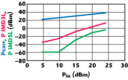
Figure 10 Two-tone test results for PA2 at 1 GHz with a tone spacing of 4 MHz.
A two tone inter-modulation distortion measurement was carried out at 1 GHz. The separation between the two carrier tones was the same as before, 4 MHz. The IMD3 at 10 dB back off the P1dB was -32 dBc and the output IP3 was 50 dBm. The results are shown in Figure 10.
Comparison of Both Power Amplifiers
The measured results indicate that PA2 is more stable than PA1, because there is less variation in the results obtained for PA2 (except at 1.8 GHz), while major differences are seen in the results at different frequencies for gain and PAE for PA1. This could possibly be because the design for PA1 was without feedback and was totally dependent on its bias and input matching network for stability. The second reason could be the thermal conductivity of the SiC substrate (PA2), which is higher than Si (PA1). At Vd = 28 V, Pmax at 700 MHz for PA1 is 18 W, which is 10 W for PA2 at Vd = 48 V. The average maximum output power obtained from PA2 is almost equal to the power out designated by the manufacturer of the transistor, while a higher power than the designated one was obtained for broadband at almost one third of the bandwidth in the case of Si-based GaN HEMT (PA1). The PAE for PA1 is above 40 percent at all measured frequencies (and 66 percent at 200 MHz) comparing to PA2, for which it varies between 10 and 37 percent. The PA2 had the advantage of operating at a higher drain bias of Vd = 48 V. A wider frequency band, high power gain, PAE and unconditional stability was achieved without feedback using a Si-based transistor (PA1) compared to SiC-based GaN HEMT (PA2). The linearity of both amplifiers is also comparable.
Conclusion
Two single-stage broadband power amplifiers, using two different GaN HEMT technologies, have been designed and fabricated. Both amplifiers showed good performance in output power, PAE, gain and linearity for the frequency band of 0.7 to 1.8 GHz. It is interesting that a wider bandwidth, higher power, gain and PAE were achieved for a GaN transistor grown on a Si substrate (PA1). Since GaN on Si is a cost-effective solution, together with high quality performance, it is the future technology of choice, due to the cost advantage of large diameter silicon wafers. In PAR and the communication sector, the major hindrance for adoption of GaN technology compared to its rival LDMOS is its cost, which is gradually decreasing by introducing GaN on Si. The results of the Si-based GaN technology indicate that these devices have strong potential to replace the same present Si LDMOS designs in the telecommunications sector. This technology can become the first choice in many other RF and microwave applications.
Acknowledgment
The authors acknowledge the subsystem group (previously the microwave group) at the Swedish Defense Research Agency (FOI-Linköping) for providing the laboratory facilities and participating in technical discussions.
References
1. Y.F. Wu, A. Saxler, M. Moore, R.P. Smith, S. Sheppard, P.M. Chavarkar, T. Wisleder, U.K. Mishra and P. Parikh, “30 W/mm GaN HEMTs by Field Plate Optimization,” IEEE Electron Device Letters, Vol. 25, No. 3, APRIL 2004, pp. 117-119.
2. A. Maekawa, T. Yamamoto, E. Mitani and S. Sano, “A 500 W Push Pull AlGaN/GaN HEMT Amplifier for L-band High Power Application,” 2006 IEEE MTT-S International Microwave Symposium Digest, pp. 722-725.
3. A. Wakejima, T. Nakayama, K. Ota, Y. Okamoto, Y. Ando, N. Kuroda, M. Tanomura, K. Matsunaga and H. Miyamoto, “Pulsed 0.75 kW Output Single-ended GaN-FET Amplifier for L/S Band Applications,” Electronics Letters, Vol. 42, No. 23, November 2006.
4. J.H. Kim, J.H. Moon, Y.Y. Woo, S.C. Hung, I.D. Kim, J.J. Kim and B.M. Kim, “Analysis of a Fully Matched Saturated Doherty Amplifier with Excellent Efficiency,” IEEE Transactions on Microwave Theory and Techniques, Vol. 56, No. 2, February 2008, pp. 328-338.
5. J.H. Moon, J.H. Kim, I.D. Kim, J.J. Kim and B.M. Kim, “A Wideband Envelope Tracking Doherty Amplifier for WiMAX Systems,” IEEE Microwave and Wireless Components Letters, Vol. 18, No. 1, January 2008, pp. 46-48.
6. P. Colantonio, F. Giannini, R. Giofre` and L. Piazzon, “High-efficiency Ultra-wideband Power Amplifier in GaN Technology,” Electronics Letters, Vol. 44, No. 2, January 2008.
7. Y.F. Wu, S.M. Wood, R.P. Smith, S. Sheppard, S.T. Allen, P. Parikh and J. Milligan, “An Internally-matched GaN HEMT Amplifier with 550 W Peak Power at 3.5 GHz,” 2006 IEEE International Electron Devices Meeting Digest, pp. 1-3.
8. J. Gassmann, P. Watson, L. Kehias and G. Henry, “Wideband, High-efficiency GaN Power Amplifiers Utilizing a Non-uniform Distributed Topology,” 2007 IEEE MTT-S International Microwave Symposium Digest, pp. 615-618.
9. S.C. Hong, Y.Y. Woo, I.D. Kim, J.H. Kim, J.H. Moon, H.S. Kim, J.S. Lee and B.M. Kim, “High Efficiency GaN HEMT Power Amplifier Optimized for OFDM EER Transmitter,” 2007 IEEE MTT-S International Microwave Symposium Digest, pp. 1247-1250.
10. K. Yamanaka, K. Mori, K. Iyomasa, H. Ohtsuka, H. Noto, M. Nakayama, Y. Kamo and Y. Isota, “C-band GaN HEMT Power Amplifier with 220 W Output Power,” 2007 IEEE MTT-S International Microwave Symposium Digest, pp. 1251-1254.
11. S. Azam, R. Jonsson and Q. Wahab, “Designing, Fabrication and Characterization of Power Amplifiers Based on 10 W SiC MESFET and GaN HEMT at Microwave Frequencies,” Proceedings of the 38th European Microwave Conference, 2008, pp. 444-447.