
An active integrated antenna (AIA) may be defined as a system in which an active device, usually a transistor, is closely integrated within an antenna, using a minimum of intervening circuitry. In recent years, AIAs have been considered a useful approach for improving performance and reducing size in front-end wireless communications applications. The antenna is not only a radiating element, but also a part of the input or output tuning circuits, and may present optimised impedances that are non-standard and partly reactive. In contrast to the design methodology of the conventional 50? interface, an AIA can be regarded as an amplifying active microwave circuit that has free space termination as its input or output.
In a transmitting context, attempts have been made to use AIAs to improve the power-added efficiency (PAE) of power amplifiers. Several novel high efficiency PA designs have been proposed by using AIAs to perform harmonic tuning.1–5 In these articles, the antennas are attached directly to the active devices and play a role in terminating higher order harmonics at the PA’s output to achieve high output power (Pout) and high PAE.
Here, a CAD-oriented approach is discussed to optimise the fundamental load impedance in the design of a class-F power amplifier used as a transmitter in an AIA. A 2 × 2 coupler at the input stage is used in designing the input matching circuit by showing the effect of various load impedances on the input reflection coefficients. To demonstrate the principle, the case study of a 1.6 GHz, class-F power amplifier AIA design for wireless communications is presented. A published design10 for the antenna structure has been chosen, but has been integrated with a different transistor.
AIA Amplifier Design
Class-F operation is a well-known technique for improving the PAE of RF power amplifiers. It uses a multi-resonator to control the harmonic waveforms so that the drain voltage waveform (ideally) becomes rectangular and the drain current waveform becomes half sinusoidal, thereby reducing the DC power dissipation and increasing efficiency. This requires an impedance optimised at the fundamental, a low impedance at the even harmonics and a very high impedance at odd harmonics. A simple method is to interpose a quarter-wave length line between the drain and the final load and to design the latter to have the lowest possible impedance at all harmonics above the fundamental.
For the AIA harmonic tuning, it is convenient to use the same technique. This has been done by others,3–5 where, to obtain class-F operation, the second and third harmonics are shaped through the input resistance of the antenna. This technique allows these harmonic resistances to be almost zero at twice and three times the design frequency, so that harmonic power is efficiently suppressed from radiation by the antenna. In addition, the input impedance of the antenna at the fundamental frequency (fo) should be equal to the optimum load impedance (Zopt) at fo of the amplifier for maximum PAE and Pout. In this design approach, an output matching circuit is eliminated because the antenna impedance is directly transformed to the Zopt for maximum efficiency, thus decreasing the circuit complexity and power losses.
In this CAD-oriented approach, due to the intrinsic active device nonlinear behaviour, the PA design is based on large-signal simulation. The class-F power amplifier was designed and optimised at 1.6 GHz using Agilent Technologies’ Advanced Design System (ADS). Following selection of a suitable output power and operating frequency range, the active device selected was the TriQuint CLY5 power GaAs field effect transistor (FET). For a simple design, it is desirable to use a device like the CLY5, which does not include built-in matching circuits, other than unavoidable parasitics, within the package. Even with CAD tools, it is a very difficult problem to optimise all aspects of the design in one pass. No exact synthesis technique is known for shaping a patch antenna to achieve prescribed impedances at a set of harmonically related frequencies. However, it is feasible to use the method of References 2 and 3, whereby the fundamental impedance can be kept reasonably close to optimum, while higher resonances of the patch can be separated as much as possible from harmonics of the operating frequency, so that the input resistance of the patch remains low at the harmonics. This may, of course, be a realistic target only for the first few harmonics, which fortunately dominate the efficiency optimisation. Feedback effects on input impedance at harmonic frequencies is a complex issue. In this case study, the procedure starts by initially optimising the fundamental load impedance only, and this value is used in optimising the input match, again initially neglecting harmonic frequency feedback.
The nonlinear model of this device (which was provided by the device manufacturer), and harmonic balance simulation, including the first five harmonics, were used in the simulation. The drain bias voltage, Vds, was 5 V, while the gate bias voltage, Vgs, was set to be –2.25 V, so that DC drain current is 155 mA. Figure 1 shows the DC characteristics of the device and the selected quiescent bias point.
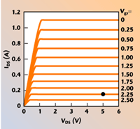
Fig. 1 DC characteristics of the device and the selected quiescent bias point.
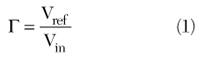
A set of large-signal S-parameters is usually required for matching network design in PAs. However, the measurement of these S-parameters is not well defined. An alternative method is to derive the reflection coefficients of the active device from measurements of the voltages of the incident and reflected waves. In this AIA scenario, only the input reflection coefficient (?in) needs to be obtained, because of the elimination of the output matching. A 2 × 2 simple coupler was inserted at the input stage of a class-F harmonic load-pull measurement design circuit (which was in ADS’s amplifier design guide), in order to measure ?in of large-signal S-parameters of the nonlinear model. The simulation circuit with a coupler for the input matching design is shown in Figure 2. In this circuit, the coupler is connected between a signal generator and the active device, in order to make a measurement of the incident voltage (Vin) incoming from the source and the reflected voltage (Vref) reflected back from the active device. It should be noted that the coupler is not intended to be a realizable hardware component, but is defined in software as the operation of converting actual current and voltage into equivalent forward and reverse wave components. The Gin of the transistor is then calculated according to the defining equation
The principle of this CAD load-pull measurement circuit design is to obtain the Zopt at the fundamental design frequency of the PA with a class-F biasing operation at fo for maximum PAE and Pout (the accepted power to the load or antenna), using an algorithm to vary the fundamental load impedances which are contained in a one-port device as S11 data. In fact, the algorithm is provided by the ADS package, arbitrarily setting a center point and radius for a circle on the Smith chart and also setting the number of points on the circle (making sure the generated circle is fully inside the Smith chart). Each point of the circle gives an individual value of the load impedance. The optimum load impedance can be obtained by changing the location of the circle on the chart. In addition, the source and load impedances at harmonic frequencies were defined arbitrarily as 50?. These assigned values are somehow sub-optimal. Thus, the obtained PAE and Pout from this simulation design are not finalized and the design can be used as a starting point when the one-port block is replaced by the antenna, which should hopefully provide the correct harmonics load impedances. The input reflection coefficients were also simulated as a function of the output load impedances for maximum power and efficiency. Due to the dependence between the input reflection coefficient ?in and the load reflection coefficient ?load of the two-port device, the advantage of this proposed design approach is that it simplifies the considerations of designing the output matching circuit and the simulation only aims to obtaining Zopt. Once the Zopt with the required output power and efficiency was obtained, the corresponding ?in with this Zopt value was also calculated so that the input matching circuit could be designed accordingly with the aid of the Smith chart.

Fig. 2 Harmonic load-pull simulation circuit with a coupler.
Under the biasing condition previously mentioned, the ?in value when Zopt was optimised was found to be 6.049–j10.096 ?. With the help of the Smith chart tool, an input matching circuit with two lumped elements was plotted and replaced the coupler at the input stage. Discrete components could be used for the matching network because these components have been characterised well enough at the lower microwave communication frequencies. A modified measurement circuit with optimal components’ values is shown in Figure 3.

Fig. 3 Harmonic load-pull simulation circuit with input matching.
After introduction of the input matching, the PAE and Pout of the PA were dramatically improved, while the Zopt was still found to be 16.049–j10.096 ? with the same input power level. Once the Zopt value was set, microstrip lines were required to connect these components together. An Ultralam 2000 substrate with ?r = 2.55, thickness T = 1.524 mm, metal thickness Tm = 0.035 mm and tan ? = 0.0019 was assumed. Figure 4 shows the design circuit connected using microstrip lines with optimal lengths and widths of MLINs, MTEEs and STUBs. One-tune swept harmonic balance analysis, with load impedances at harmonic frequencies set at 50? and the optimum load impedance at the fundamental frequency set as 16.049–j10.096, was employed. The output power Pout and the PAE characteristics from the active device versus input driving power at 1.6 GHz are shown in Figure 5. The PAE of the transistor reaches 69.7 per cent with an input power level of 18 dBm. The corresponding performances are 27.81 dBm output power and 9.85 dB gain. Table 1 shows the power amplifier’s performances with the same input power level versus various load impedances at harmonic frequencies.

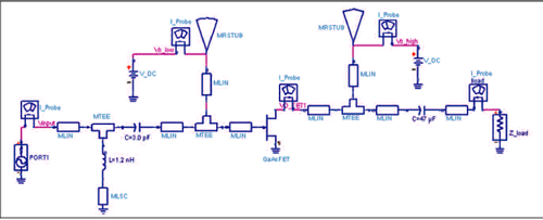
Fig. 4 Simulated circuit model with optimum load.

Fig. 5 Simulated performance of the power amplifier; (a)Pout and PAE, and (b) higher harmonic level.
Various antenna types could be chosen for the radiating element of the AIA, including patch antennas2 and planar inverted-F antennas.4 To realise class-F operation with the AIA concept, this study followed the approach of References 3 and 5 and adopted the same antenna geometry as in Radisic, et al.,5 which used a circular-sector microstrip patch antenna, as shown in Figure 6. It had been checked that the antenna shown in Radisic5 was actually fed at the edge of the patch, and a quarter-wave transmission line was believed to have been added to transfer the antenna’s input impedance to the drain output of the active device. It is also necessary to point out that the operating frequency of the whole active antenna in Radisic5 was chosen to be near the first resonant frequency of the patch. The same antenna design procedure was used in this study. However, the active device chosen was different. The optimum fundamental load was found to be 16.049–j10.096?. It was also discovered that an output matching network would have to be included6 between the drain and antenna input port. In order to avoid this network, the antenna size had to be increased in order to be able to make a match near the patch antenna’s second resonance. Figure 7 shows the simulated input impedance for an antenna radius of 45 mm, the intended operating frequency being 1.6 GHz. The antenna’s impedance at the first three harmonic frequencies is also shown in Table 2.
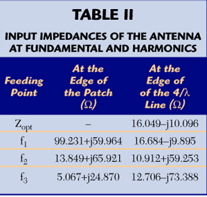

Fig. 6 Layout of the circular-sector microsctrip antenna.
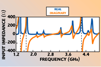
Fig. 7 Simulated input impedance of the circular-sector microstrip antenna with a radius of 45 mm.

Fig. 8 Final simulated model integrated with the antenna data.
The antenna was incorporated in the class-F PA simulation as a one-port device containing the S-parameter data from 0.2 to 9 GHz. The final simulated model, including the antenna data, is shown in Figure 8. The amplifier performance with the integrated antenna as harmonic loading is shown in Figure 9. It is obvious from the data that an increase in PAE, output power and power gain at 18 dBm input power have been obtained. These results demonstrate an approach to show how the harmonic loading of the actual antenna can contribute to the PA performance as compared to the simple harmonic loading (that is without the actual antenna data) introduced by the ADS package. Figure 10 shows the simulated drain voltage and drain current waveforms. They show deviations from the ideal case waveforms, but a performance improvement has nevertheless been obtained. These deviations are believed to be due to the parasitic reactive elements of the nonlinear model of the active device, particularly the packaging parasitics at the drain and in the common (source) lead. A check was made to show that including more harmonics would have little effect on these results. Similar waveform deviations were observed in Radisic,5 where four harmonics were used for the simulation work.
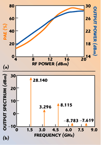
Fig. 9 Improved simulated performance of the power amplifier; (a) Pout and PAE, and (b) higher order harmonic level.
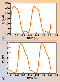
Fig. 10 Simulated drain current (a) and drain voltage (b) waveforms.
Conclusion
A simple CAD-oriented approach to optimise load impedance at the fundamental frequency for the application of the active antenna concept was described. The design method and procedure were presented. In addition, one design example at an operating frequency of 1.6 GHz was demonstrated to verify the design principle. It was confirmed that performance could be substantially enhanced in an active integrated antenna. n
References
1. Y. Qian and T. Itoh, “Progress in Active Integrated Antennas and Their Applications,” IEEE Transactions on Microwave Theory and Techniques, Vol. 46, No. 11, November 1998, pp. 1891–1900.
2. V. Radisic, Y. Qian and T. Itoh, “Novel Architectures for High Efficiency Amplifiers for Wireless Applications,” IEEE Transactions on Microwave Theory and Techniques, Vol. 46, No. 11, November 1998, pp. 1901–1909.
3. Y. Chung, C.Y. Hang, S. Cai, Y. Qian, C.P. Wen, K.L. Wang and T. Itoh, “AlGaN/GaN HFET Power Amplifier Integrated with Microstrip Antenna for RF Front-end Applications,” IEEE Transactions on Microwave Theory and Techniques, Vol. 51, No. 2, February 2003, pp. 653–659.
4. S. Liw and G.A. Ellis, “Planar Inverted-F Antennas as an Inverse Class-F Termination for Wireless Applications,” IEEE Antennas and Wireless Propagation Letters, Vol. 2, 2003, pp. 250–253.
5. V. Radisic, Y. Qian and T. Itoh, “Class-F Power Amplifier Integrated with Circular-sector Microstrip Antenna,” IEEE MTT-S International Microwave Symposium Digest, 1997, pp. 687–690.
6. T. Itoh, G. Haddad and J. Harvey, RF Technologies for Low Power Wireless Communications, John Wiley & Sons Inc., Somerset, NJ, 2001, pp. 219–223.