
Commercial and military satellites require cost-effective ICs that meet stringent high-reliability standards. In addition, they need to provide distinct advantages that allow designers to advance satellite technology in order to meet changing needs, especially in terms of cost (weight, power), reliability (number of transmission lines, radiation tolerance, redundancy) and performance (including the ability to enhance opportunities for flexible payload designs using phased-array antennas or a switch matrix). Silicon on sapphire (SOS) is inherently a great match for these business and technical constraints, and is currently available in high-volume, high-yield commercial production.
A form of SOS technology that uses ultra-thin films, UltraCMOS™ technology is an extension of RF complementary metal-oxide-semiconductor (CMOS) technology that enables the manufacture of high-performance RF devices. Particularly important for satellites, this technology has low gate capacitance and fully depleted devices, which enables high speeds at low power. These devices also greatly improve linearity as compared to typical silicon on insulator (SOI) and GaAs technologies, and they offer 2 kV typical Human Body Model (HBM) electrostatic discharge (ESD) protection. Presently in high-volume production for commercial applications, UltraCMOS technology meets high-reliability and environmental requirements for operating in space and yields tend to be comparable to other CMOS processes.
Process Advantages for Satellites

Figure 1 Bulk Si process devices (top) have higher parasitics because of the thick layer of Si while UltraCMOS process devices utilize a thin 1000 Å Si layer.
CMOS technology’s advantages of low power and ease of integration are well known.1 UltraCMOS technology is a CMOS technology where a 50 to 100 nm silicon film is formed directly on a sapphire substrate. When properly processed, this provides for fully depleted devices with little or no body charge under the gate (see Figure 1). As compared to traditional CMOS processing, UltraCMOS offers the advantage of faster devices with reduced power loss, excellent linearity, high isolation and no kink effect. For satellite applications, this proves to be particularly valuable in the avoidance of single-event effects.
The insulating, single-crystal alumina properties of sapphire allow the manufacture of dielectrically-isolated transistors. This improves power handling as compared to other process technologies, such as GaAs. Also, since it is still a CMOS technology, it offers high yields, on-chip logic and low defect density. UltraCMOS processing can be classified as SOI technology. However, in most SOI technologies, a thin layer of insulating dielectric material is required between the MOSFET device and the silicon layer. While this approach reduces the effects of the parasitic capacitances and leakage currents, it significantly limits device performance. UltraCMOS technology does not suffer the effects of a semiconducting silicon (Si) substrate.
Cost

Figure 2 Weight is critical in satellite design — every Kg of load costs approximately $30,000 to launch.
For satellite designers, issues of cost, weight and power consumption are closely entwined. Satellites must generate their own power while in space. Most are powered by solar cells (although some deep-space satellites use nuclear energy). When a satellite’s power needs to grow, it requires more solar cells and power supplies. In addition, power generates heat, which is very difficult to counter in a vacuum in space. This translates to more weight, which immediately means more cost. Estimates are that every additional kilogram of weight adds $30,000 to the launch costs (see Figure 2). A current estimate of launching a very small satellite puts the cost at $21 to $28 M.2

Figure 3 An UltraCMOS device can integrate this discrete device PLL in a single 68-lead CQFJ package.
The most effective way to address weight is with monolithic integration. Due to the insulating nature of the sapphire substrate, this technology has the ability to integrate RF, mixed signal analog, passive and digital functionality on the same device. Figure 3 shows the functional blocks of an UltraCMOS 3.5 GHz delta-sigma modulated fractional-N PLL frequency synthesizer IC (Peregrine Semiconductor). This type of single-chip implementation of a phase-locked loop (PLL) allows for easier control thanks to short lead lines, less weight, a smaller footprint and higher reliability. The PLL device pictured in Figure 3 features a 10/11 dual modulus prescaler, counters, a delta-sigma modulator and a phase comparator. Counter values are programmable through either a serial interface or directly hard-wired. UltraCMOS shows great promise for increased integration, especially of digital functionality, and higher integration directly addresses weight concerns as well as improved reliability.
After considering launch costs, the design focus often shifts to minimizing power usage in space (in order to reduce the number of solar panels and power supplies). To put power consumption in context, a typical planetary satellite uses 500 W to 10 kW of power, while a typical commercial LEO/GEO satellite uses 2 to 20 kW. It is important for satellite designers to select the most efficient devices for their designs in order to keep these numbers as low as possible. As an example, an UltraCMOS prescaler, for instance, uses 1/14th the power of a comparable GaAs part due to its low-power CMOS design (see Table 1).

One way to minimize power consumption is to select devices with the best power handling efficiency. In the case of RFICs, that also means finding parts that offer high linearity. Input third-order intercept point (IIP3) is a key specification that measures linearity. Because UltraCMOS features fully depleted operation, the devices tend to have high linearity and attenuation accuracy. Generally speaking, digital step attenuators (DSA) manufactured using this technology demonstrate linearity that is about 8% better than comparable GaAs parts. For example, one UltraCMOS DSA features +34 dBm peak output power at 1 dB compression (P1dB) typical, +52 dBm IIP3 typical and flat performance from 1 MHz to 3 GHz. This device is used in many communications payloads and in phased-array applications. It is a simple monolithic design that replaces design types using PIN diodes or discrete GaAs switches.
In another example, an UltraCMOS single-pole double-throw (SPDT) switch is often selected for use in phased-array applications in satellites because of its linearity and lower power. This switch demonstrates an 18 percent improvement in linearity over typical GaAs products with an IIP3 of +60 dBm at 6 GHz (see Figure 4).

Figure 4 By selecting RFICs with higher linearity, satellite designers can reduce power consumption and launch costs.
Broadband operation offers another cost-saving opportunity for satellite designers. The cost to qualify a component for use in space can range from 100s of thousands to a million dollars, so a component that operates across a wide bandwidth offers the advantage of being ‘future proof’ when design changes occur. An UltraCMOS prescaler that operates from 3 to 13.5 GHz is well suited for a range of applications. And, since this IC is made in a high-volume commercial process, its quality control and production lifetime can be better than devices that are manufactured in non-commercial flows.
Reliability
For space applications, reliability is extremely important. Besides excellent design and tight manufacturing tolerances, some ways to improve reliability are to reduce the number of control lines, minimize the number of components through integration and maintain the necessary radiation tolerances. Because it can include digital control logic, UltraCMOS is fast becoming a process technology of choice for space applications, especially those that use phased-array antennas (which require high levels of control).
Eliminating wires and lines inside a satellite reduces weight and removes potential points of failure, which improves reliability. Unlike GaAs, UltraCMOS can easily incorporate serial addressability, so that only two to three lines are required to control the device. Without this feature, it is necessary to directly wire each line on any device. Without serial addressability, designers have to run multiple lines with line drivers across sections of the satellite (recognize that a satellite can be the size of a truck). For example, in one UltraCMOS DSA, this feature allows designers to address up to eight separate DSAs (using addresses 000 – 111).
Radiation tolerance is a basic necessity for the reliable devices that must be used in space applications. UltraCMOS does not use bulk CMOS (which is subject to parasitics), so it has a natural resistance to ‘single event effects.’ Commercial submicron Ultra-CMOS also handles total dose radiation well enough that no special design or process modifications are needed for the vast majority of radiation-hardened products used in space.
Radiation environments require RFICs to be immune to the single event effects that occur when a particle from a cosmic ray or a high-energy proton travels through the die and impacts performance. Because UltraCMOS has only a very thin layer of silicon, it is much more resistant to these issues than traditional CMOS. There are two types of single event effects: Single-event upsets of a logic gate (non-destructive errors that can be corrected by rewriting to the logic gate) and single-event latchups (hard errors that can be destructive to the device). Primarily an issue for bulk CMOS designs, single event latchups can cause a short circuit, requiring at minimum a power down to recover. (Keep in mind that resetting can take days in space applications.) Products manufactured using UltraCMOS do not contain the bulk parasitics found in regular CMOS devices, making latchup impossible. As a result, products come with guaranteed immunity to single-event latchup, and they demonstrate an exceptional natural tolerance to single-event upsets.
Performance
In satellite designs, increased performance leads to faster data handling. This is beneficial for commercial applications, yielding more revenue-generating opportunities, and military applications, because delivering more data can allow scanning in more areas and/or reduce the need for satellites or equipment. Some of the key performance metrics for improving performance in satellite RFICs include ESD performance, phase noise and high voltage handling.
Most satellites use state-of-the-art ESD controls, but they can still benefit from components with good ESD protection. UltraCMOS offers this kind of additional protection, with up to 4 kV HBM ESD protection with low parasitics.
Phase noise is perhaps one of the most critical performance parameters for satellite RFICs. Simply put: Every 3 dB improvement of phase noise can double the data handling capability of the satellite. UltraCMOS PLLs were designed to compete in tough commercial base station markets and therefore have excellent phase noise, i.e. one UltraCMOS PLL design features phase noise of -216 dBc/Hz. The potential for even better phase noise performance exists. For instance, the current generation of this product realized a 4 to 10 dB improvement over the previous generation. In addition, this part boasts low power consumption of 45 mA at 3.3 V.
Dramatic improvements such as these in phase noise performance have been applied to flexible payload systems. This trend in satellite design is moving towards in-orbit payload flexibility, which extends a satellite’s revenue-earning potential. In the past, a signal was transmitted to the satellite and then broadcast to a fixed location back on Earth. In this model, companies would buy access, but they were not really transmitting large amounts of data. With a flexible payload, the satellite can handle data on the fly, transmitting to various locations on Earth on-demand by using electrically reconfigurable (phased array) antennas rather than fixed ones. The advantage of this approach is that each independent channel beam is programmable, and it can be repeatedly assigned to new addresses. In the commercial realm, providers are able to sell more data access and be more flexible where it is sent. On the military side, more data can be processed and delivered. It also increases reliability in mission-critical applications, allowing one satellite to back up another in a fleet if necessary.
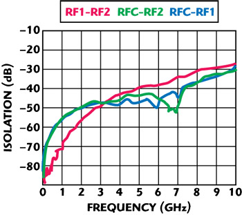
Figure 5 UltraCMOS SPDT switches can achieve 82 dB isolation at 100 MHz.
Another popular design trend in satellites is the use of a switch matrix. This type of design is made possible by high-performance solid state switches. However, these multiple radio signals also require high isolation. In the case of a SPDT switch a good target would be 70 dB isolation. With UltraCMOS, devices are being manufactured with high levels of isolation (see Figure 5). This is made possible because sapphire is a perfect insulator,3 allowing the transistors to be dielectrically isolated, which provides both latch-up immunity and high isolation. One UltraCMOS SPDT broadband switch design that is frequently used in switch matrix applications typically runs at a low IF and features 82 dB isolation at 100 MHz (see Figure 5).

Figure 6 Stacking FETs in series can enable high voltage handling.
Because of the lack of parasitics in the UltraCMOS process, RFIC designers can stack field effect transistors (FET) in a series, which allows for high voltage handling (see Figure 6). In contrast, bulk CMOS processes cannot support stacking to the same degree.
Voltage handling has been an important feature in commercial terrestrial designs, but now interest is growing in using this feature for satellite designs as well. For instance, a UltraCMOS SPDT that is used as a high-power switch in public safety radios and many other commercial applications is now being explored for use in satellite phased-array applications to replace circulators. This switch achieves 50 W P1dB, with unmatched performance by GaAs MMIC options. As an additional advantage, eliminating a circulator and replacing it with a high-power switch would allow satellite designers to save up to 2 kg per satellite.
Technology Future
Future development is expected to include further improvements in performance, such as phase noise, higher frequencies and higher integration. The use of UltraCMOS in satellite applications is growing rapidly. For many years, SOS was the technology of choice, but the purely military usage caused the technology to lose momentum. By applying a commercial technology to satellite and other high reliability markets (99.997 percent of all UltraCMOS devices have shipped to purely commercial applications), worldwide satellite systems are improved. As satellite designers work with more phased-array and communication payload designs, they can take advantage of the inherent characteristics that are made possible by the extremely thin layer of silicon and the subsequent elimination of bulk parasitics. As satellite manufacturers increase the number of transmit and receive elements and arrays (up to 10s of 1000s in one antenna), they are likely to utilize the technology’s advantages in power consumption, digital control and integration.
When RFIC designers work out the challenges before them, they will be deciding what level of integration is possible and needed, perhaps bringing RF, digital and analog all together on the same UltraCMOS chip, including input/output switches, digital/analog converters, attenuator, phase shifter and digital control. The good news is that UltraCMOS offers the cost, reliability and performance characteristics that make it future-proof for satellite design and these devices are already shipping in high volume.
References
1. R. Reedy and M.C. Comparini, “Perspective of RF CMOS/Mixed Signal Integration in Next-generation Satellite Systems,” European Microwave Week, 2003.
2. “US plan to fly small, rapidly deployable satellites faces scrutiny,” http://www.networkworld.com/community/node/27305, Network World, 04/28/08.
3. G. Imthurn, “What is Silicon on Sapphire,” http://www.psemi.com/articles/History_SOS_73-0020-02.pdf.