

At present, market demand for miniaturization of SMT components is satisfied at the expense of poorer component insertion loss and limited levels of ultimate rejection. While high Q components offer increased range and/or reduced noise figure at the system level, miniaturized components fit mechanical constraints and tight budgets. The Leadless SMT Air Cavity Filter provides an option for better balancing of design requirements between the existing extremes.
The Solution
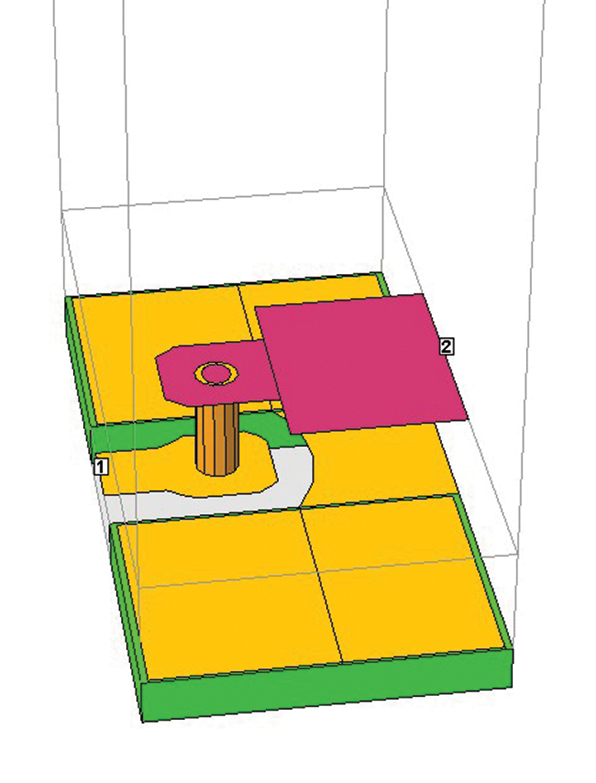
In most cases, the printed wiring board (PWB) of choice for the user’s end module is a microstrip structure consisting of a low dielectric (2 to 10) organic material. In the proposed solution (patent pending), an additional PWB is soldered to the base of the filter, which carries the RF signal from the microstrip structure to the RF pin positioned in the floor of the filter, as depicted in Figure 1. Using a planar simulator, such as Sonnet, the transition is analyzed over a wide frequency range, and its S-parameters are stored. Next, a cavity filter is designed to suit the RF specifications and then optimized between (in cascade with) the stored S-parameters at both of its ports, as shown in Figure 2. The filter is matched between two complex loads by changing the internal impedance and couplings between resonators. Correct tap points to the first and last resonators are also determined in the final steps of the design.

Between the I/O ports, the adapting PWB is filled with plated-through-holes (PTH) to ensure maximum isolation by keeping RF leakages down. RF leakage is a typical problem and the primary cause of deteriorating the ultimate rejection in miniaturized SMT filters. Assembly of the filter and PWB adaptor is accomplished using SN-96 solder, with a melting range of 221° to 229°C, so that the completed unit can be reflowed into the user’s end-product using SN-63 solder. The RF signal path transitions from a microstrip to a stripline structure to a vertical plated-through-hole, entering the cavity filter via a coaxial RF pin. The RF pin provides the filter with complete shielding from humidity, which is often encountered during PWB cleaning after the solder reflow phase.

Test Results
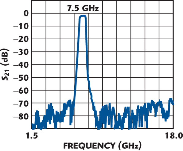
A five-pole Chebyshev bandpass filter centered at 7500 MHz with a 500 MHz equal-ripple bandwidth was built and tested. The filter was assembled and soldered to an RO4003 PWB with a thickness of 31 mils. One end of the RF pin was soldered to a loading wire, while the second end was soldered to the inner PTH conductor. The filter assembly was reflow soldered to a test fixture made of RO4003 with a thickness of 13 mils. With a ground plane spacing of 0.13" and a 3 dB bandwidth of 600 MHz, the estimated unloaded Q predicted an insertion loss at mid-band of just above 1 dB. The narrowband and wideband responses, shown in Figures 3 and 4, are in excellent agreement with predicted performance.
SMT Filters from Moderate to Large Bandwidths
Cavity (TEM) filters have limited support for moderate (> 50 percent) to large (> 100 percent) bandwidths, due to the finite close proximity of the resonators. With careful analysis and tuning of transitions, the PWB adaptor concept is viable for these wider bandwidths, but a different filter structure must be used. The approach can be extended by substituting a suspended substrate structure for the cavity structure, particularly for high pass and low pass responses. This variation is depicted in Figure 5.
Conclusion

A new transition from microstrip to cavity filters has been presented. This solution provides a platform for higher Q filters to be mounted via SMT, reducing connector count and required space. The increased ultimate rejection provides sharper roll-offs and enhanced dynamic range for systems. Broadband devices with extended Q are also possible.
K&L Microwave Inc.
Salisbury, MD
(410) 749-2424
www.klmicrowave.com
RS No. 301