
Recently I was asked, “How much GaAs do you own?” This may seem like a strange question and certainly one that I would not have even thought worthy of consideration as little as five years ago.
If like me, you remember when the principal drivers for GaAs products were phased-array radar, satellite communications and electronic warfare (EW), then the idea of owning a piece of GaAs may not have entered your mind either. Considering this today and broadening it to the wider RFIC context, however, this simple question actually probes quite deeply into the nature and trends of current business.
In the everyday world, microwaves are no longer synonymous with re-heating food, and the most obvious example of RFICs in your pocket is the ubiquitous mobile phone. But even that contains not one, but at least two microwave bands with associated chips, notably PAs, switches and low noise amplifiers (LNA). Many will also contain a Bluetooth transceiver. In addition, almost all laptops bought in the last year will have an 802.11 interface, usually again with PAs and switches, which, depending on the bands and possible use of multiple antennas, can amount to three or four chips with other features such as Bluetooth becoming more standard.
Many homes now have a wireless Internet router with devices similar to the PCs to complete the radio link. Printers, cameras and a host of other domestic appliances are now sprouting wireless connectivity. If you have satellite TV, there is an LNB containing six or so low noise X-band devices as well as other RFICs in the set top box. There are also devices to transmit signals to the multitude of TV sets in homes today. Going slightly further a field, my car has a built-in Bluetooth interface while others have short-range radar, GPS, security tags and tracking systems.
Against this multitude of consumer applications for RFICs, it seems that the industry and particularly the GaAs segment is at a crossroads. The traditional requirements for RFICs in military, avionics and high value commercial markets have not gone away. They just have not really grown that much. In fact, where there was once a civilian spin off from military advances, the position is becoming reversed and military procurement agencies are looking for commercial off-the-shelf (COTS) hardware to address dwindling budgets.
From the manufacturer’s perspective, the commercial realities of supporting the consumer market are quite different to those of the traditional military and specialist product business areas. It is not just a matter of volume; it is also time to market, rolling cost reduction programs and product evolution. These are diametrically opposed to the relatively long lead-time, highly controlled design process and long-term product support requirements of military customers.
Faced with these design and production differences, never mind the widely varying customer base, many manufacturers are recognising a need to focus on one market or the other. While the attention is on the newer high volume commercial markets, those who choose to stick to the traditional have an opportunity to rejuvenate fortunes.
Trends on RF and Microwave ICs
By going to trade shows, conferences and reading journals, one sees a significant move away from advocating highly technical advances like fabrication enhancements and increases in the cut-off frequency or power density. Instead, titles and eye-catching bullets more frequently highlight lower cost, increased functionality or wide application. Of course, there are still notable and ongoing improvements in technological areas. They are, however, less publicized as they are now very commercially sensitive, and secrecy can be even more stringent than for military programs.
Unlike the past, the technological trends are less visible and while it may seem like a cliché to say that the three most important trends are cost, cost and cost, it really is true. Of course, costs come in many forms and that is the interesting part. However, cost, translating into customer value, is still the cornerstone of each of the themes I shall be considering in this article. They include:
- Actual – materials, processing, die shrinkage, advanced modeling and better design.
- Functional – increased functions per die, expansion of the application horizon per die and marriage of mixed technologies on the same die.
- Non-semiconductor – thermal management, packaging and mixed technology integration.
Actual
In response to demand, the industry has seen a significant shift to larger and larger wafers. This trend has been most visible in the silicon world but, in GaAs, for example, while there are still forecasts and budget models built on four-inch wafer figures, the reality is that the majority of parts are now made on six-inch wafers. The significant increase in usable area and hence die per wafer compared to the relatively fixed cost of manufacture makes this an obvious trend.
However, with significant technical challenges in growing eight-inch or larger GaAs bulk material and the lower incremental area increase in going from six- to eight-inch wafer production, there is little prospect of a further jump in wafer sizes in the near future.
Another major trend is the relentless progress of silicon processing and its effects on the RFIC business. While the primary focus of these efforts is in the computer and data applications industry, there are significant side effects in the RF world. The tremendous push towards geometry shrinkage produces transistors with higher and higher frequency capability. It is just a matter of time before this potential is used for actual RF products.
On the more immediate front, the move of mainstream computer chips to sub-90 nm fabrication lines releases fully depreciated manufacturing capacity to address lower volume RF products. For example, for Gen 6 LDMOS devices, companies like NXP have adopted RF power device processing to be made on CMOS lines, putting further downward pressure on the cost per watt of these devices.1
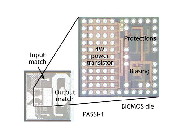
Similarly, the handset market is seeing increased competition from silicon devices to established GaAs HBT solutions. Figure 1 shows a BiCMOS power transistor die with integrated biasing and protection circuits, flip-chipped on a passive silicon die with partly integrated input and output matches.2
In the HBT and GaAs PHEMT areas, there has been tremendous progress in reducing the cost of materials like MBE wafers, decreasing fabrication cycle times and reducing processing steps. In epitaxial growth, where conventional wisdom dictated inevitable expense from the long cycle times and necessary batch processing through high vacuum equipment, the premium suppliers have combined significant economies of scale with good old manufacturing excellence to consistently reduce costs while maintaining or even increasing uniformity.
Such suppliers have worked with customers to consistently achieve significant price reductions. Also, fabrication engineers have almost halved mask and process steps in recent years for lean manufacturing and better utilisation of expensive capital equipment.
In a similar trend, leading manufacturers such as Skyworks and Anadigics have announced combining PHEMT and HBT processing on a single BiFET wafer.3 This opens up the possibilities of expanded functional integration in handsets by combining a single supply, high power density HBT, PAs with a low power consumption and low loss PHEMT antenna switches on a single chip.4,5 There is still some way to go on key issues like isolation and linearity, but this process advancement plays into my next theme in the cost reduction arsenal.
Functional
Just like many other markets, after an initial reduction in price for new devices or technologies, there comes a point when further price reduction becomes uneconomic and manufacturers look to retain sales revenue by increasing the function for the same price. The RFIC market is no exception and has certainly reached that point in some sectors. Here, however, because of different relative strengths, the various fabrication technologies approach the issue differently.
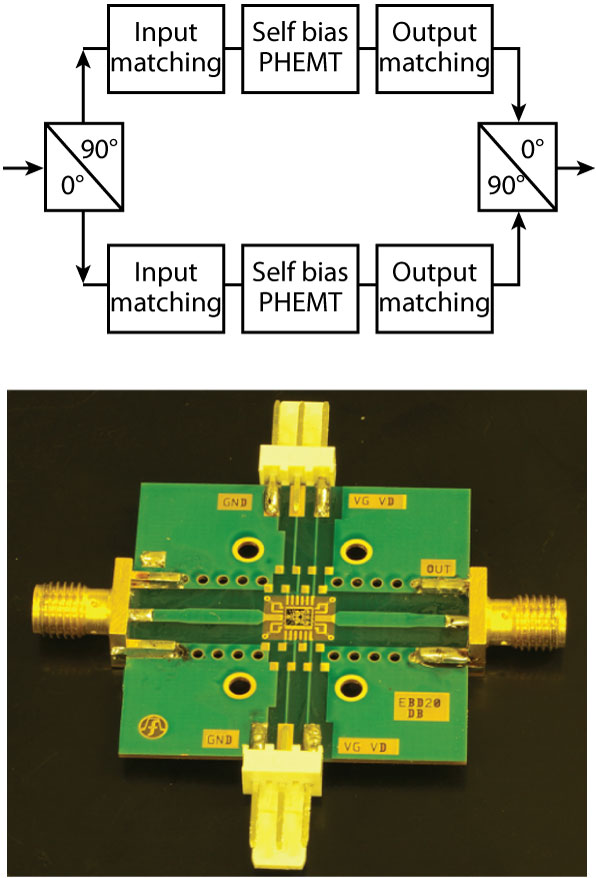
The Filtronic FMA3017 shown in Figure 2 is a good example of higher integration in the GaAs PHEMT field. While d-mode devices have generally shown superior performance over the e-mode equivalents, they have always suffered from the need for a negative bias voltage.
In most LNA applications, there is still demand for balanced stages, so most designs require two FETs and two hybrid couplers. The Filtronic part integrates both FETs with the couplers and the bias decoupling needed for single supply, self-bias operation into a 4 x 4 QFN. Compared to the board space and cost of the individual parts, this elegant solution illustrates maintaining market share while giving customers better value for their money.
Other examples of this increase in functionality can also be seen in related technologies. QinetiQ and BAE Systems recently published a complete millimetre-wave 62 to 65 GHz transceiver on a chip.6 Similar advances and complexity were also demonstrated in SiGe technology.7
While such high levels of integration are relatively modest in GaAs FET technology, it shows that reliable process and accurate modeling are enabling the realisation of higher-level functions. However, these are very small steps compared to the functional integration achievements in CMOS technologies. Combining the microwave frequency performance that is now possible in CMOS with the traditional capabilities of IF and digital processing produces true systems on a chip (SoC).
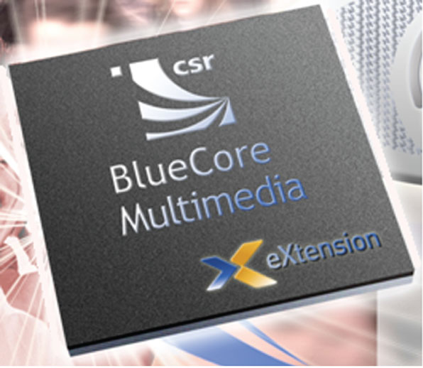
For example, the Cambridge Silicon Radio (CSR) BlueCoreX family offers single chip radio and baseband ICs for Bluetooth 2.4 GHz systems, as shown in Figure 3. The low output power of the Bluetooth standard allows huge chunks of the RF and digital requirements to be integrated onto a single 0.13 mm CMOS chip.
Increase in chip functionality is very much a matter of perspective. For GaAs FET-based devices, at high frequencies, integration is in its infancy. There are recognised difficulties in DC biasing of complex circuits and traditional RF matching elements are quite small, so design approaches are often miniature versions of thin film counterparts.
In contrast CMOS, SiGe and HBT approaches use many transistors, more like op-amps and other low frequency ICs. Complete system integration certainly favours technologies that are compatible with logic. Combining analog with digital capabilities eases integration with system control functions as well as the continual incorporation of RF functions into more and more advanced DSP.
Non-semiconductor
Looking at costs at all levels of the manufacturing process inevitably leads to consideration of the ‘other’ costs. In the power transistor market, the heat sink material of choice now is copper, with lower cost and higher thermal conductivity than traditional materials.8 Similarly, the illusion of the hermetic package has been broken at last and various plastic air cavity and over-molded packages are now in the market, removing the relatively expensive ceramic frames and lids. This change really opens the way for further integration of functions into power devices. After all, it was pointless considering a bigger die than necessary when the package was so expensive, but changes in packaging technology enable new solutions.
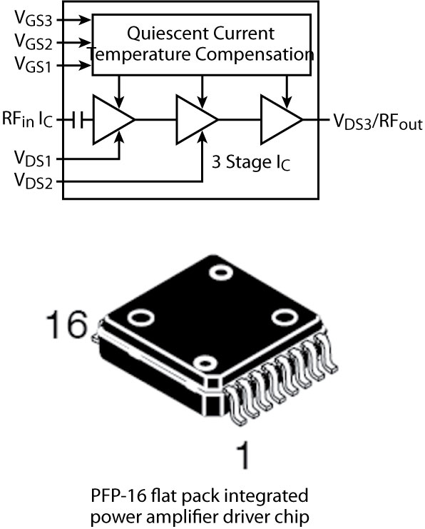
One example of this can be seen in Figure 4, a Freescale base station LDMOS IC driver. Here, a class AB driver amplifier chain is integrated with other bias control circuits into a single surface-mount package. A diminutive 7 x 9 mm surface-mount package holds up to three amplifier stages and delivers up to 15 W peak RF output. Compared to the cost of individual parts and associated board space, this is a significant cost saver and just a sign of things to come in the integrated power device market.
In low power RF modules, the progress in integration and footprint reduction has been tremendous. Several manufacturers now offer packaged solutions for the whole RF front end of phones, wireless routers and similar products.9 These advances follow the increased functionality ideas discussed earlier, but in a very different way. Rather than focus on the die level, these solutions are at the package level; by freely mixing active and passive technologies, silicon, SiGe and GaAs dies, as well as surface-mount parts, appropriate cost performance targets are met.
With this ‘Optimum Technology Matching’ strategy, there is even a trend towards less functionality per die. For example, handset PA die are minimised to just the active components with other functions off-loaded to lower cost passive only substrates in Si or GaAs. This makes sense as long as the fabrication capacity can support such measures, but it does tie up relatively expensive processing equipment on low margin products. With growth still projected in the RFIC market, the future will be for alternatives to present integrated passive die.
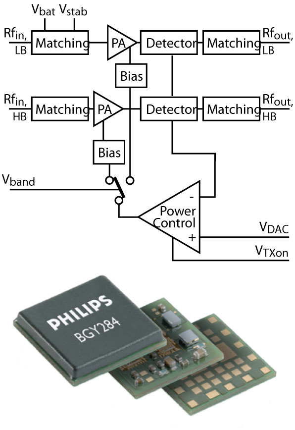
The NXP example in Figure 5 clearly shows mixed technology integration in the otherwise featureless plastic SMT package. Here, GaAs HBT technology for the PA is combined with Si PASSI substrate for off-chip matching and decoupling, Si BiCMOS for drivers and control functions integrated with SMT parts on a low cost organic substrate.
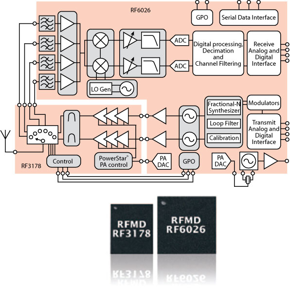
There are similar products from other manufacturers, with perhaps the most advanced being from RFMD, as shown in Figure 6. This further integrates SAW and baseband devices for a system in a package (actually two packages) and complete RF-to-digital functionality.
Advances in packaging technology play a significant role in this trend. With SMT parts now as small as 0201 and innovative uses of organic substrates with hot vias and vertical integration concepts, there is every indication that higher functionality can be achieved with this approach, independent of advances at the die level.
Other Business
Some see a tremendous future in wide bandgap semiconductor-based circuits for RF power applications. Indeed, the attractiveness of the physical properties is indisputable and, particularly in the case of GaN, progress has been remarkable, eclipsing earlier hopes for high voltage GaAs.10,11 Just like early GaAs developments, the early adopters are the military, where the benefits can be applied to immediate requirements.
However, commercial products are likely to be further away in that highly cost-competitive market. Early claims of greater than 10 W/mm power densities have almost been halved recently, and even then it seems that because of thermal management issues these devices require wider gate-to-gate pitches than GaAs. With the relative high cost and small size of GaN substrates and using the more practical comparison of watts per mm2, the advantages of GaN compared to established high power technologies, at least for the cellular base station market, are not as clear as initially thought.
Conclusion
To answer my original question, I certainly own more RF semiconductor real estate than I realised. Also, as with so many good questions, the interesting part is not so much the numerical result, but more in the way you get to an answer. With mobile handset production predicted to reach one billion this year, uptake of more advanced products in the developing world and demand for greater wireless connectivity almost everywhere, there is clearly scope for further growth. For me, the major trend is that manufacturers are taking the magic out of RF product design, enabling innovation and greater market penetration through wider adoption of the technology.
References
- I.I. Blednov and J. van der Zanden, “High Power LDMOS Integrated Doherty Amplifier for W-CDMA,” 2006 Radio Frequency Integrated Circuits Symposium Digest.
- A. van Bezooijen. “Over-temperature Protection by Adaptive Output Power Control,” 2006 European Conference on Wireless Technology.
- “Skyworks Favors Hybrid BiFET Designs,” Compound Semiconductor Magazine, September 2006.
- M. Sun, et al., “A High Yield Manufacturable BiFET Epitaxial Profile and Process for High Volume Production,” 2006 CS MANTECH Conference Digest, pp. 149–152.
- M. Shokrani, “InGaP-Plus™: A Low Cost Manufacturable GaAs BiFET Process Technology,” 2006 CS MANTECH Conference Digest, pp. 153–156.
- J.R. Powell, P.D. Mundy, W.H. Tang, R.C. Hunt and D.J. Gunton, “MMIC and Module Design and Performance for Millimetric Transceiver Front-ends for Transport Applications,” 2006 IEEE MTT-S International Microwave Symposium Digest, pp. 1497–1500.
- T. Yao, et al., “65 GHz Doppler Sensor with On-chip Antenna in 0.18 mm SiGe BiCMOS,” 2006 European Conference on Wireless Technology.
- L. Hamel, “Low Cost Thermally Improved RF Power Transistor Packages,” IWPC Workshop, High Efficiency, High Linearity Semiconductor Devices for Base Station PAs, November 2005.
- J. Neal, “The RF Semiconductor Evolution: From Single Components to Systems Solutions,” Microwave Journal, Vol. 48, No. 2, February 2005, pp. 22–30.
- A. Maekawa, T. Yamamoto, E. Mitani and S. Sano, “A 500 W Push-pull AlGaN/GaN HEMT Amplifier for L-band High Power Application,” 2006 IEEE MTT-S International Microwave Symposium Digest, pp. 722–725.
- K. Inoue, “A High Gain L-band GaAs FET Technology for 28 V Operation,” 2005 IEEE MTT-S International Microwave Symposium Digest.
 Richard Ranson received his BSc and PhD degrees from the University of Leeds, England, in 1976 and 1979, respectively. He has worked in the microwave electronics industry for more than 25 years, first for Philips in the UK, then in the US, primarily for Watkins Johnson. He returned to the UK in 1996, joining Filtronic Comtek as subsystems engineering director and later engineering director for the Integrated Products Division. He is a visiting professor at Leeds University and is presently working as an independent consultant. He has extensive experience in military and commercial radio systems, successfully completing a wide variety of projects ranging from specialist radar receivers, EW and intelligence gathering radios, instrumentation such as spectrum analysers and high volume products for cellular communications.