
PRODUCT FEATURE
A 17 to 27 GHz GaAs MMIC Gain Block Amplifier from Multiple Sources
Mimix Broadband
Webster, TX
 A GaAs MMIC three-stage gain block amplifier covering the 17 to 27 GHz frequency range has been developed that features the option of individually biasing the three stages or biasing them in parallel to achieve different performance characteristics. Following initial production at a US-based foundry, this part has now been prototyped at a low cost six-inch Asian-based foundry, with essentially similar performance. The company plans to have multiple foundry sources for its high volume parts to assure rapid supply at competitive prices. The XB1000 gain block amplifier features a typical small-signal gain of 22 dB with a noise figure of 3 dB when operated as a low noise amplifier (LNA) (with the three stages biased in parallel). Higher output power, along with a slightly degraded noise performance, is achieved when the amplifier is operated as a buffer amplifier (input stages biased independently from the output stages).
PERFORMANCE
Used as an LNA, the linearity is sufficient to meet the European Telecommunications Standard Institute's (ETSI) dynamic range requirements. Under normal LNA biasing the power output at the 1 dB compression point (P1dB) is +13 dBm and the output third-order intercept (OIP3) is +23 dBm while maintaining a 3 dB noise figure across the full 17 to 27 GHz frequency band. However, when biased for optimum power output (Vd1,2 = 5.5 V, Id = 180 mA) the amplifier typically achieves +19 dBm at P1dB, and a +29 dBm OIP3 with only a small degradation in noise performance. Maximum input power is 0 dBm.
Figure 1 shows the XB1000 amplifier's power output and gain performance vs. input power at 17 GHz. Small-signal gain (S21) typically runs 22 dB with a gain flatness of ±1 dB. Typical input and output return losses (S11 and S22) are 10 and 8 dB, respectively.
|
|

Maximum supply voltage and current is 5.5 V and 180 mA, respectively. At Vd = 3 V and Vg = 0.3 V (small-signal operation) the typical supply current (Id) is 90 mA. Figure 2 shows the device's typical S-parameters vs. frequency under small-signal conditions. Note: this process has a higher breakdown voltage than Foundry 1, allowing operation at 6 V. However, both devices are normally operated at 5.5 V with similar performance.
|
|

FABRICATION
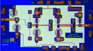
The 2.66 x 1.50 mm XB1000 MMIC is fabricated using a 0.15 µm GaAs pseudomorphic high electron mobility transistor (PHEMT) device technology and is based on electron beam lithography to ensure high repeatability and uniformity. Electrical performance is ensured by 100 percent on-wafer RF, DC and noise figure testing. In addition, there is 100 percent visual inspection to MIL-STD-883 Method 2010. Figures 3 and 4 illustrate the uniformity of gain and noise figure performance over 12 different wafers. These data are from the initial production run from Foundry 1 and shows the typical variation to be expected over process variations for GaAs PHEMT devices using e-beam defined gates. The chips feature surface passivation for protection and provide a rugged part. Backside via holes and gold metallization allow either a conductive epoxy or eutectic solder die attach process.
 |
|

APPLICATIONS
The XB1000 three-stage gain block amplifier is best suited for millimeter-wave point-to-point radio applications, local multipoint distribution systems, satellite communication systems and very small aperture terminal use. In addition, the device is used as part of a sub-circuit that includes an image-reject mixer on the company's XR1000 receiver.
CONCLUSION
A GaAs MMIC three-stage gain block amplifier is now available and can function equally well as a front-end LNA or buffer amplifier depending on the bias applied to the individual stages. The device achieves high yields and good reproducibility for use in today's millimeter communications systems. Additional information is available at the company's Web site at www.mimixbroadband.com.
Mimix Broadband,
Webster, TX (281) 526-0536.
Circle No. 302