
A 2.7 GHz RF/IF Gain and Phase Detector
Analog Devices Inc.
Norwood, MA
Gain and phase are fundamental properties of all radio systems. The need to measure these parameters is exemplified through the ubiquitous use of vector analyzers. The AD8302 gain/phase detector integrated circuit was developed to accurately measure the gain ratio (dB) and phase difference between two signals, one of which may be a known reference signal.
HISTORY
Over the years, a broad range of RF power level detectors and variable gain amplifiers have been introduced by the RFIC industry to implement measurement and control functions. Discrete diode detector circuits have been replaced with simple integrated circuit logarithmic (log) detectors, eliminating the need for complex temperature compensation and calibration circuitry. Log detector products that are now available allow users to measure signals with dynamic ranges approaching 100 dB at frequencies of up to 500 MHz for receiver signal strength indication (RSSI) applications, and with 70 dB dynamic range at frequencies of 2.5 GHz for transmit signal strength indication (TSSI) applications.
The increasing desire for higher speed wireless data provided by the new 2.5G/3G cellular systems and emerging broadband wireless access systems requires the implementation of more complex, higher order, modulation schemes. These modulation schemes, including 8-PSK, 64-QAM and CDMA (QPSK), have signals with varying crest factor. The peak-to-average level of the signal varies, making the task of power level detection even more difficult.
As a result, a new detector topology was developed to perform the analog computation of the root mean square value of the input signal. The AD8361 TruPwr detector is the first product using the new topology and provides a measurement that is virtually independent of crest factor variations.
A NEW TYPE OF DETECTOR
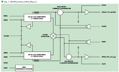
All previously available detectors provide an output that is proportional to the incoming signal. The AD8302 device is a new type of detector that enables users to measure the ratio (difference in decibels) between two input signals. The AD8302 IC integrates two logarithmic detectors, each with a 60-dB dynamic range, plus a linear multiplier and circuits used for amplitude and output scaling, onto a single IC. A block diagram is shown in Figure 1.

Two independent input signals (or an input and a known reference signal) may be applied to Va and Vb . The output represents the differences in log-amplitude (gain or loss) and in phase between the two inputs. The amplitude signal output is scaled to 30 mV/dB and the phase output is scaled to 10 mV/degree.
The AD8302 IC uses log amplifiers instead of rms (TruPwr) detectors because limiter outputs associated with the log amplifiers can be used to monitor phase. The limiter outputs are fed to an on-chip linear multiplier that computes the phase difference. In order to understand how to measure signals with high crest factors the transfer function of the log amplifiers must be examined.
Their transfer function is given by
Vout = Vscale * log (Vin /Vx )
Vscale is the logarithmic slope and is specified in mV per dB. Vx is the intercept of the amplifier. This is generally regarded as the point at which the logarithmic slope crosses the X-axis, and its variation is the main source of errors within the log amplifier.
The AD8302 has two closely matched log amplifiers on the same die, so the intercept points or error terms are closely aligned. These errors are then subtracted by the amplitude current differencer.
The response for the two log amplifiers a and b can be written as
Vout = Vscale1 * log (Va / Vx1 ) Vscale2
* log (Vb /Vx2 ) = Vscale * log (Va /Vb )
if Vscale1 = Vscale2 and Vx1 = Vx2
Changes in logarithmic response for complex signals with different crest factors are minimized since both log amplifiers are closely matched on the same die.
Figure 2 shows the AD8302 detector's functional block diagram. On-chip bias circuitry sets the scaling of the input and output levels. The bias circuit also provides an accurate, stable 1.8 V reference.
For an amplitude measurement VMAG is nominally set by
VMAG =
(30 mV/dB) * 20log (Va /Vb ) + 900mV
The maximum dynamic range is 60 dB, with the midpoint set at 0.9 V. This provides the user with a 0 to 1.8 V signal swing. The log amp dynamic range has been set to provide a 30 to +30 dB range; in order to achieve the full dynamic range the reference channel is required to be set to 30dB.
For a phase measurement VPHS is nominally set by
VPHS = 10 mV/deg
* (Qa Qb 90) + 900 mV
The range for phase measurement is limited to 180° with the midpoint (90°) set at 0.9 V. This provides the user with a 0 to 1.8 V signal swing. If a 360° range is required, the user must determine independently which quadrant the phase is in. Figure 3 shows the gain and phase detector's output characteristics.

PERFORMANCE
The accuracy of the AD8302 detector is dependent on a multitude of factors, including the relative difference between the two input signals in both amplitude and phase at the frequency of interest (RF or carrier frequency), the signal bandwidth at the chosen carrier frequencies and the device operating temperature range.
Performance data for the AD8302 is provided over the popular cellular frequency ranges -- 900 MHz, 1.8 GHz and 2.2 GHz. The part performs accurate amplitude measurement up to 3 GHz and accurate phase measurement (over a limited dynamic range) out to 2.7 GHz.
Figures 4 and 5 show data taken on several devices at 900 MHz, 1.8 GHz, 1.9 GHz and 2.2 GHz, all superimposed on the same graph. In both cases the A channel is used as the reference and is set at 25 dBm, while the B channel is swept from 25 dBm to 35 dBm and 0° to 360°, respectively.
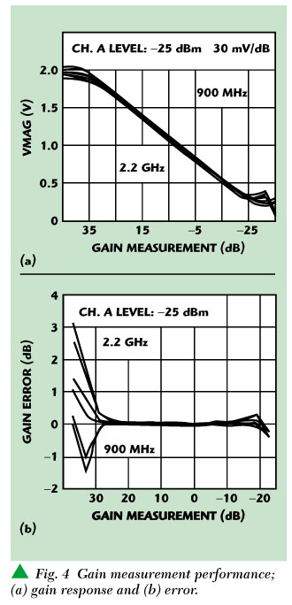

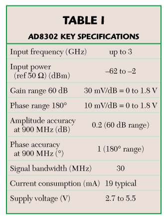
The gain measurement shows less than 0.2 dB error over a greater than 40 dB range, and less than 1 dB over the entire 50 dB dynamic range at 900 MHz. The phase measurement shows less than 1° error at 900 MHz over the full 0° to 180° range. However, at higher frequencies the dynamic range is reduced as the phase approaches the neighborhood of 0° or 180°. Table 1 summarizes the AD8302 key specifications.
AVAILABILITY
The AD8302 is fabricated on a high performance 25 GHz ft silicon bipolar process. The device is packaged in a 14-lead thin shrunk small outline (TSSOP) package and is fully specified over a 40° to +85°C temperature range. Samples and evaluations boards are currently available.
Analog Devices Inc.,
Norwood, MA (781) 329-4700.
Circle No. 303